
Step Conductivity Measured with the Proximity-Induced Superconducting Pair Correlation
Hasegawa and Kato Groups
The recent discovery of monolayer (ML) superconductivity revived the research on one-atom-thick metal layers formed on semiconductor surfaces. Electronically decoupled from the substrate, the metallic overlayers hold an ultimately-thin two-dimensional (2D) electron system, and combined with the broken inversion symmetry, they exhibit various fascinating features, such as Rashba spin-split surface states and valley spin polarized states. For these 2D systems, atomic steps on the substrate, whose presence is ubiquitous and unavoidable, play a significant role in the transport. Usually, for the characterization of electrical conductivity, an electrical current is injected from one side of the object and the transmitted one is detected in the other side. It is, however, technically very difficult to measure transport on such nano-scale structures. Here, we report on microscopic measurements of the electrical conductivity through a single ML-high step on a 2D metallic layer by inducing the superconducting pair correlation through the proximity effect, and by detecting its signal in tunneling spectra measured by scanning tunneling microscopy and spectroscopy (STM/STS).
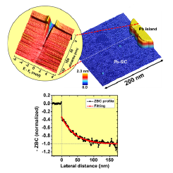
Fig. 1. (upper panel) 3D-rendered STM image showing an interface between an 8-ML Pb island and a SIC phase formed on a Si(111) substrate. A characteristic striped pattern can be seen in the SIC phase. (inset) Color-coded 200 tunneling spectra taken along the line from the Pb island to the SIC phase. (lower panel) ZBC profile around the SN interface. The red line is a fitted exponential function with the decay length of 40.5 nm.
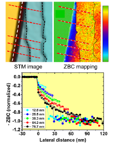
Fig. 2. (upper left) STM image of a Pb island formed on a SIC-phase-covered Si(111) substrate. The edges of the Pb islands and the steps of the SIC phase are highlighted with white and black dashed lines, respectively. (upper right) ZBC color map of the same area. (lower) ZBC profiles across the SN interface and the step edges measured along the red lines drawn in the STM and ZBC images. The length written on each plot is the terrace width measured along the corresponding line. The whitish-colored lines are theoretical curves calculated with the Usadel equation.
The propagation of the pair correlation from a superconductor / normal metal (SN) interface into the normal metal has been investigated by using STM/STS. Near the interface in the normal metal, the single particle spectrum shows a dip at the Fermi energy (EF), which is a good measure of the superconducting pair correlation. Through spatial mapping of the density of states (DOS) at EF with nanometer spatial resolution, one can learn how the pair correlation is distributed in the normal metal. In general, the pair correlation decays with distance from the SN interface. By placing a surface step within the decaying area we can investigate how the superconducting coherence is affected by the presence of steps and through the comparison with theoretical analysis we can estimate the conductivity through that.
We investigated the conductivity of a striped incommensurate (SIC) phase, a ML Pb-induced structure formed on Si(111) surface, which is a 2D normal metal at our measurement temperature (2.15 K). Figure 1 is an STM image showing an 8 ML Pb island on an SIC phase. Tunneling spectra taken along the line, shown in the inset, indicate a superconducting gap in the Pb island and no gap in the SIC phase far from the island. In the SIC phase near the island a suppressed gap, induced by the proximity effect, can be seen. The depth in the DOS at EF, which corresponds to zero-bias conductance (ZBC), decays exponentially with distance from the interface (the decay length ~ 40 nm), as shown in the lower panel of Fig. 1. From the decay length, the conductivity through the SIC phase was estimated using the Einstein relation as 1.87 mS/□. The estimated conductivity is larger than the one measured by 4-probe method (0.77 mS/□). The larger conductivity is reasonable since the separation of the 4-probe method (20 μm) is much larger than the step separation and therefore the measured area includes the steps whereas ours do not.
To measure the step conductivity, we investigated the spatial distribution of the pair correlation around steps of the normal-metal layer close to superconducting islands. The left panel of Fig. 2 is an STM image showing 22 ML high Pb island (yellow) formed on a stepped SIC phase (light blue). The ML-high steps on the SIC phase are marked with black-dashed lines. The spatial mapping of ZBC taken in the same area is presented in the right panel of Fig. 2. In the conductance map the Pb island is colored green, which indicates zero ZBC and fully gapped superconductivity there. The 2D metallic layer far from the Pb islands is colored yellow, indicating no gap. The area surrounding the Pb islands is colored blue to red, implying a reduced DOS at EF due to the proximity effect. Since a downward step edge is close to the island and the terrace width of the SIC area is less than the decay length, the decaying behavior of the proximity effect is strongly modified by the presence of the step edge. The bottom panel of Fig. 2 displays several cross-sectional ZBC profiles taken in the areas with various terrace widths.
In order to obtain the conductivity through the surface step we calculated the ZBC profiles using the Usadel equation and compared them with experimental results. For the calculation we considered a model composed of three regions: superconductor / normal metal / normal metal. In the model, we introduced the conductivity ratio through a step and metallic layer as a parameter. From the fitting the ratio was estimated as 10.9 ± 3.9 μm-1. The ratio indicates that the contribution of the step resistance to the total surface resistance is quite significant. In the case of the stepped area shown in Fig. 2 (~90 nm step separation corresponding to the tilting of 0.20°), which was observed on a nominally (111)-oriented substrate, the step resistance contributed almost 50% of the total resistance in the direction perpendicular to the step edges.
References
- [1] H. Kim, S. -Z. Lin, M. J. Graf, Y. Miyata, Y. Nagai, T. Kato, and Y. Hasegawa, Phys. Rev. Lett. 117, 116802 (2016).