
Double Carrier Transport in Electron-Doped Region in High-Mobility Thin-Film Black Phosphorus FET
Osada Group
Black phosphorus (BP) is a layered material which was extensively studied in the 1980s because it was a single-element semiconductor with higher mobility than silicon or germanium. In the past a few years, BP has again attracted a great deal of attention as one of post-graphene atomic layer materials. It shows high performance as a field effect transistor (FET) material; much larger on/off ratio than graphene and higher mobility than transition metal dichalcogenides. It is known that thin-film BP is degraded by photochemical reaction under oxygen and water atmosphere, so that techniques to avoid the degradation are important to obtain high quality thin films. Using high quality samples, the Shubnikov-de Haas (SdH) oscillations and the quantum Hall effect of two dimensional (2D) carriers have been studied. However, most of preceding studies were performed in negatively gated (hole-doped) region. In this work, we have achieved the highest Hall mobility ever reported in thin-film BP, and observed clear SdH oscillations, which indicate double carrier transport in positively gated (electron-doped) region.
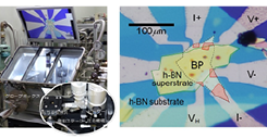
Fig. 1. (left) Exfoliation and transfer system for building atomic layer heterostructures. (right) Microscope image of thin-film BP FET device.
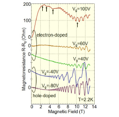
Fig. 2. Magnetoresistance of thin-film BP FET under several gate voltages.
The samples were prepared by the mechanical exfoliation and dry transfer techniques in the grove box to avoid degradation. First, a thin-film BP flake with the thickness of 15-20 nm is fixed on an atomically-flat hexagonal boron nitride (h-BN) flake on the SiO2/n+-Si substrate. Next, it is partially covered by a smaller h-BN flake. Electrodes are formed on the edge of this top h-BN flake by the lithography process in the atmosphere. Since the measured region in BP layer is sandwiched by two h-BN layers, we can avoid the degradation and improve carrier mobility. Using this simple method, we have achieved the Hall mobility of 6,000 cm2/Vs and 5,800 cm2/Vs at 4.2 K for holes and electrons, respectively. These values are comparable to the reported highest mobility.
In the negatively-gated (hole-doped) side, we have observed negative magnetoresistance (MR) due to weak localization and SdH oscillations with clear spin splitting. The carrier density estimated from the SdH period is well proportional to the gate voltage with small correction of charge neutrality. This fact indicates that a single 2D hole gas is formed in the inversion layer.
In contrast, anomalous transport behaviors have been observed in the positively gated (electron-doped) side. The gate voltage dependence of conductance showed an anomalous shoulder structure. In the gate voltages below it, normal behaviors, the negative MR and single SdH oscillation, were observed like the hole-doped side. In the gate voltages above it, the MR turned to positive and saturated accompanied by slow and fast SdH oscillations. The summation of carrier densities estimated from two SdH periods coincides with the density expected from the gate voltage. These facts clearly suggest the existence of two closed Fermi surfaces. In addition, the overall shape of MR can be qualitatively explained by the two carrier model.
The appearance of the second Fermi surface in high positive gate voltages is explained by the carrier population onto the second subband. In thin-film BP FETs, the 3D conduction band splits into 2D subbands due to finite thickness and strong gate electric field. Since the present BP sample is rather thick (15-20 nm), the subband separation is considered to be small, so that electrons easily populate on the second subband. The present result demonstrates to control the subband configuration by the gate voltage in BP FETs.