
Nondestructive Visualization of Breakdown Process in Ferroelectric Capacitors Using in situ Laser-Based Photoemission Electron Microscope
Okazaki and Kobayashi Groups
HfO2-based ferroelectrics are one of the most actively developed functional materials for memory devices because of its high scalability and compatibility with complementary metal-oxide-semiconductor (CMOS) technology and with back-end-of-line (BEOL) process [1]. In HfO2-based ferroelectric devices, dielectric breakdown is a main failure origin during repeated polarization switching. Elucidation of the breakdown process may broaden the scope of applications for the ferroelectric HfO2.
In situ laser-based photoemission electron microscope (laser-PEEM) has emerged as a powerful technique for studying dynamic processes in materials and devices at the nanoscale. By a laser with an energy comparable to the typical work function of materials, we can observe a bulk electronic structure over the depth of 50 nm [2]. This allows to reveal the chemical-state distribution in a dielectric embedded through a top electrode, nondestructively.
This report presents nondestructive analyses of HfO2-based ferroelectric capacitors using a laser-PEEM system with an in situ voltage application and characterization system.
We fabricated crossbar-type HfO2-based metal-ferroelectric-metal (MFM) capacitors on an N+ Si substrate as shown in Fig. 1. We used Hf0.5Zr0.5O2 with 10-nm thickness as a ferroelectric layer which is sandwiched by TiN with 30-nm thickness.
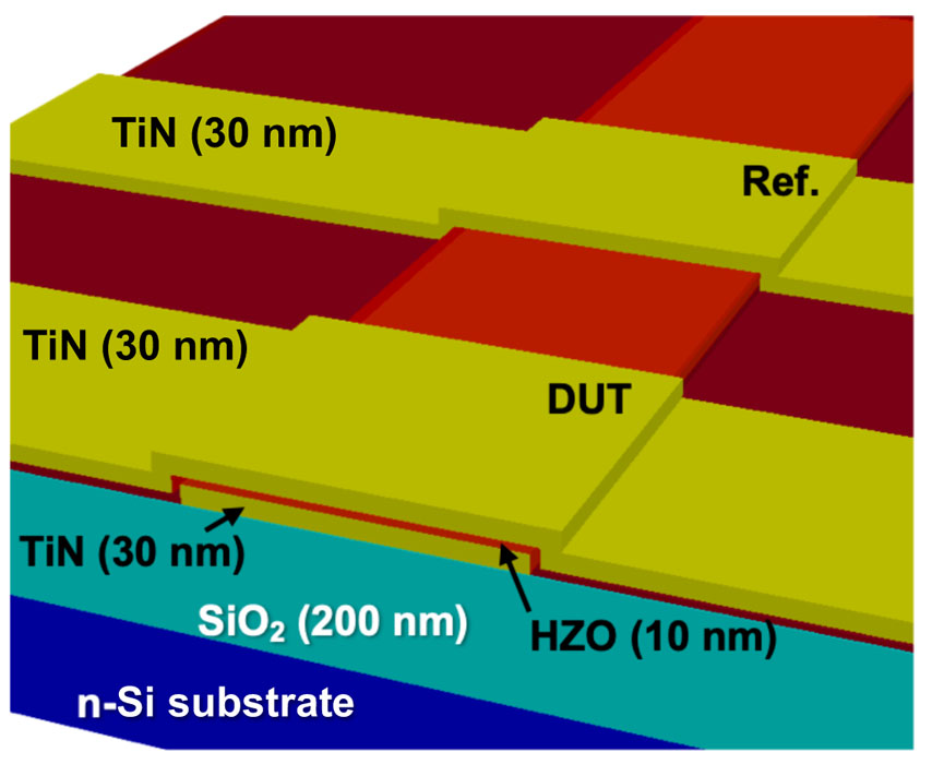
Fig. 1. Structure of the sample used for in situ laser-PEEM measurements. The values in brackets indicate the thick- ness of each film. DUT and Ref. indicate device under test and reference capacitor, respectively.
Figure 2(a) shows cycling characteristics of leakage current measured in our in situ laser-PEEM system. The leakage current began to increase above the detection limit from 1 × 10⁶ cycles. Then, the leakage current reached a local maximum at 4 × 10⁶ cycles, which corresponds to a soft dielectric breakdown (SDB). After that, the MFM capacitor was completely metalized at 7.4 × 10⁶ cycles, which corresponds to hard dielectric breakdown (HDB). This leakage current behavior during the application of cycling stress has been reported as that of typical of MFM capacitors with HZO [3]. This indicates that the waveform was applied to the MFM capacitor as designed in the source measure unit implemented in our PEEM system and also suggests that damages caused by laser irradiation during the image acquisitions can be regarded as negligible.
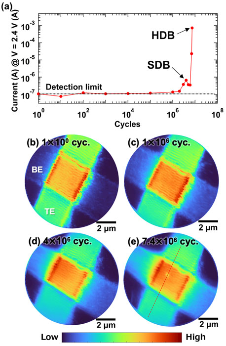
Fig. 2. Breakdown process visualized by in situ laser-PEEM. (a) Leakage current at 2.4 V on return of voltage sweep as a function of stress cycle. (b–e) Dependence of detailed PEEM images focused on the device under test on the number of cycling stresses.
Figures 2(b)–(e) show PEEM images taken after 1 × 100 cycle, 1 × 10⁶ cycles, 4 × 10⁶ cycles, and 7.4 × 10⁶ cycles, respectively. We found no significant difference between the PEEM image after 1 cycle of the square wave application and that after 1 × 10⁶ cycles, except for an increase in intensity from the bottom electrode (BE). However, after applying 4 × 10⁶ cycles, the PEEM image shows a slight increase in intensity at the corner of the MFM capacitor. From the PEEM image after HDB (Fig. 2(e)), a low- intensity spot was clearly observed near the center of the capacitor. The appearance of this spot just after the occurrence of HDB indicates that this spot is the conduction filament responsible for HDB. The result that the HDB spot was observed in the flat region is reproducible for the samples with the same dimension. This is because the electric field concentration near the edge of BE is suppressed by the voids incidentally formed at both ends of BE.
Figures 3(a) and 3(b) demonstrate that the HDB spot clearly observed by laser-PEEM is not found in the scanning electron microscope (SEM) image. This indicates that significant structural changes, such as a hillhock formation due to dielectric breakdown induced epitaxy (DBIE) of the top electrode, did not occur. It is also shown that laser-PEEM can observe changes in electronic states deeper than the probing depth of SEM. Furthermore, laser-PEEM can even investigate the electronic states in the regions where HDB and SDB have occurred. The ability to nondestructively observe not only the device topography but also the DOS distribution that dominates the functionality of materials will be indispensable for the research and development and mass production of devices that implement functional materials.
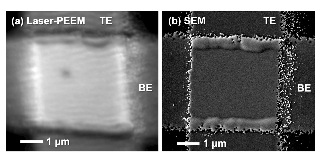
Fig. 3. Comparison of micrographs acquired by laser-PEEM and SEM. (a) PEEM micrograph after HDB, which is a magnified image of Fig. 2(e). TE and BE indicate the top and bottom electrode, respectively. (b) SEM micrograph after HDB of the sample from the in situ laser-PEEM experiment. The acceleration voltage was set to 4 kV.
In summary, we have proposed in situ laser-PEEM as a tool for observing the breakdown process of HfO2-based MFM capacitors. We observed an increase in photoelectron intensity in a region of the MFM capacitor with the onset of SDB. This corresponds to a precursory defect enhancement of HDB, which has not been clearly observed in previous TEM studies. Furthermore, we have clearly visualized the post-HDB breakdown spot. Ability of laser-PEEM to visualize the DOS distribution will be a key technology for accelerating the control of properties of functional materials and their implementation in CMOS circuits, thereby shortening time to market.
References
- [1] M. H. Park, Y. H. Lee, T. Mikolajick, U. Schroeder, and C. S. Hwang, MRS Commun. 8, 795 (2018).
- [2] Y. Okuda, J. Kawakita, T. Taniuchi, H. Shima, A. Shimizu, Y. Naitoh, K. Kinoshita, H. Akinaga, and S. Shin, Jpn. J. Appl. Phys. 59, SGGB02 (2020).
- [3] K. Y. Chen, P. H. Chen, R. W. Kao, Y. X. Lin, and Y. H. Wu, IEEE Electron Device Lett. 39, 87 (2018).