
Nonvolatile Magnetothermal Switching Induced by Flux Trapping in Sn-Pb Solder
PI of Joint-use project: Y. Mizuguchi
Host lab: Tokunaga Group
Host lab: Tokunaga Group
High-performance and high-density electronic devices require improvement of thermal management, especially thermal switch technology for controlling heat flow. Spintronic multilayer films [1] and superconductors [2] can control their thermal conductivity (κ) using only a magnetic field (H) without the mechanical motion. However, neither spintronic nor superconducting materials achieved nonvolatile magnetothermal switching (MTS). This study shows nonvolatile MTS in commercial Sn-Pb solder and discuss the origin of its nonvolatility.
We used commercially available flux-core-free solder Sn45-Pb55 (mass ratio Sn : Pb = 45:55, φ1.6 mm, TAIYO ELECTRIC IND. CO., LTD.). The chemical composition and surface of Sn45-Pb55 solder was investigated by scanning-electron microscope and energy-dispersive X-ray spectroscopy, revealing that the Sn45-Pb55 solder is a completely phase-separated composite. Thermal conductivity (κ) was measured using the Physical Property Measurement System (PPMS, Quantum Design) with the four-probe steady state method. Specific heat (C) was measured using PPMS by a relaxation mode. Magnetization was measured using a superconducting quantum interference device magnetometer on the Magnetic Property Measurement System (MPMS3, Quantum Design) with a VSM mode. We performed magneto-optical (MO) imaging at Tokunaga laboratory to observe magnetic flux trapping of Sn45-Pb55 solder in superconducting state [3]. The H dependence of the MO images at 2.5 K was observed, and all the images were temperature difference images at 2.5 K (superconducting state) and 8 K (normal state), and then normalized to the 8 K images.
Figure 1(a) displays the H dependence of κ at 2.5 K. After zero field cooling (ZFC), κ shows a low value of 10 WK-1m-1. However, when the magnetic field is increased from 0 Oe to 1700 Oe, κ rises to 35 WK-1m-1. Notably, κ does not return to its initial value when the magnetic field is decreased from 1700 Oe to 0 Oe, and κ maintains a high value throughout any magnetic field process. The initial increase in κ by the magnetic field is conventionally understood to be due to the transition of Sn and Pb from the superconducting state to the normal state.
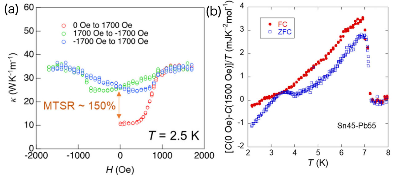
Fig. 1. (a) Magnetic field dependence of κ at 2.5 K. (b) Temperature dependence of residual specific heat estimated by C(0 Oe)-C(1500 Oe) in the form of C/T. Both ZFC and FC data are taken at H = 0 Oe ZFC and after FC under 1500 Oe, respectively.
To discuss the nonvolatility of MTS in solder, we first examine the temperature dependence of C. Figure 1(b) shows the temperature dependence of specific heat in form of C/T at H = 0 after ZFC and field cooling (FC) under 1500 Oe. The C values of the ZFC and FC data is estimated as C(0 Oe) - C(1500 Oe) to eliminate the specific heat of normal states. The ZFC data show a sharp peak due to the superconducting transition of Sn at 3.7 K and Pb at 7.2 K. However, in the FC data, while the sharp peak corresponding to the superconducting transition of Pb is observed, no peak appears near the superconducting transition temperature of Sn.
The upper panel of Fig. 2. shows the H dependence of the magnetic flux density (B) at 2.5 K. B is the sum of H and the magnetization 4πM: B = H + 4πM. Below H = 300 Oe, B = 0 G because both Sn and Pb are in the Meissner state. When H exceeds 300 Oe which is the critical field of Sn, magnetic flux penetrates and B shows a finite value. In the vicinity of the critical field of Pb at 700 Oe, the magnetic flux penetrates the entire Sn-Pb solder, and B = H. After H return to 0 Oe, a magnetic flux of about B = 400 G is trapped. The specific heat results show that the superconducting state of Sn is suppressed by FC condition. This suggests that the superconducting bulkiness of Sn is suppressed due to trapping the magnetic flux in Sn region. The lower panels of Fig. 2 show a MO images of Sn-Pb solder. Bright areas indicate positive magnetic flux, and dark areas indicate negative magnetic flux. In the initial state (i), the MO image is uniform as there is no magnetic flux in the solder. In states (ii) and (iv), the magnetic flux penetrates the entire solder. In images (iii) and (iv) at H = 0, after experiencing the magnetic field, bright or dark regions in certain clusters indicate that magnetic flux is trapped in specific region.
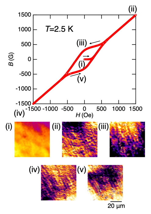
Fig. 2. The upper panel is the B-H curve at 2.5 K. The lower panels are MO images at 2.5 K. An image (i) is taken after ZFC. Images (ii) and (iv) are taken at H = 1500 Oe and H = -1500 Oe, respectively. Images (iii) and (v) are taken at H = 0 Oe after positive or negative magnetic field, respectively.
The findings of this study are summarized with the schematic images in Fig. 3. After ZFC, both Sn and Pb are in the superconducting state, resulting in low κ (Fig. 3(a)). When a magnetic field above the critical field of Sn and Pb is applied, both Sn and Pb transition to the normal state, causing κ to increase. Then, at H = 0, Pb returns to the superconducting state while Sn traps the magnetic flux, suppressing its superconductivity. Consequently, since the thermal conductivity in the Sn region remains high, the solder shows nonvolatile MTS. In this study, we focused on Sn-Pb solder as a phase-separated superconductor. Interestingly, the solder exhibited the nonvoblatile MTS, and we clarified that the flux trapping played a crucial role in this nonvolatility.
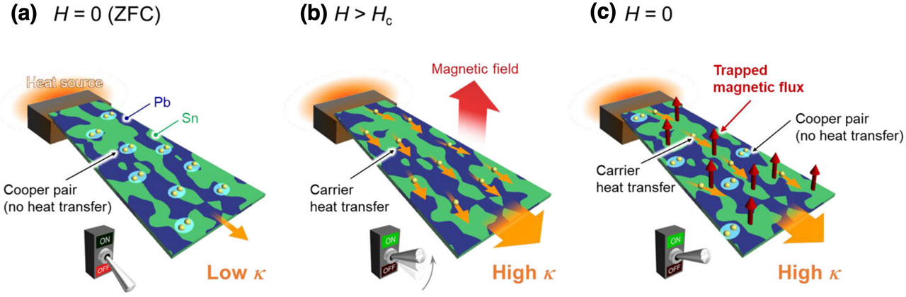
Fig. 3. Schematic images of nonvolatile magnetothermal switching in Sn-Pb solder. (a) The initial state of thermal conductivity (κ) after ZFC. (b) A state in which a magnetic field exceeding the critical field (Hc) of Sn and Pb is applied. (c) State of Sn-Pb solder in H = 0 Oe after experiencing Hc.
References
- [1] H.Nakayama et al., Appl. Phys. Lett. 118, 042409 (2021).
- [2] M. Yoshida et al., J. Appl. Phys. 134, 065102 (2023).
- [3] Y. Kinoshita et al., Rev. Sci. Instrum. 93, 073702 (2022).