
Visualizing Magnetization c Domain Structure with Heat Injection Using Atomic Force Microcopy
Otani Group
Magnetic imaging plays a crucial role in studying the magnetism of materials. Its significance has been growing with the rapid development of topological magnetic materials. For instance, the magnetic domain structure of the antiferromagnetic Weyl semimetal Mn3Sn [1] is intriguing from the magnetothermoelectric application point of view. However, the methods with enough high spatial resolution usually require costly instruments. Here, we report a simple magnetic imaging method using an atomic force microscope (AFM) with a sub-100-nm resolution, in which we measure the locally induced anomalous Nernst effect (ANE).
Figure 1(a) illustrates the concept of our method. The Joule effect of the heater causes a non-equilibrium temperature distribution in the sample nanowire. An AFM tip contact creates a local vertical temperature gradient ∇zT in a sample. The ANE is expressed as EANE = SANE(m × ∇T), where EANE, SANE, m are the electric field induced by ANE, the magnitude of ANE, and the unit vector of the magnetization, respectively. If the magnetization under the tip points to the wire width direction (the y-direction), the ANE causes a voltage along the x-direction. Therefore, the tip-induced ANE voltage represents the y-component of the local magnetization.
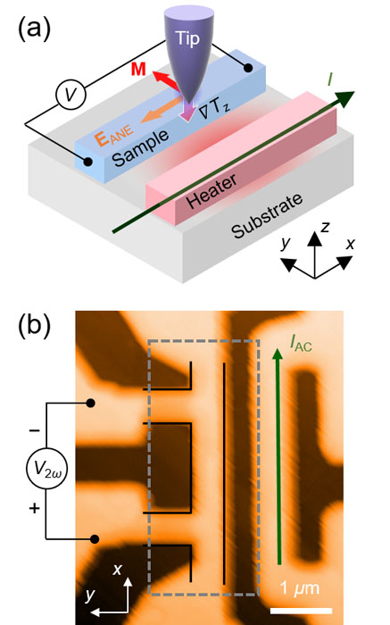
Fig. 1. (a) Conceptual drawing of magnetic imaging. (b) Device structure and electric configuration of the measurement.
We demonstrate this method on the ferromagnetic Weyl semimetal Co2MnGa that exhibits large ANE (SANE ~ 5 μV/K) [2]. The topographic image of the sample and the electric measurement configuration are shown in Fig. 1(b). We apply an alternating current to the heater and measure the voltage across the sample wire at the second harmonic frequency. We map the voltage during the scan with the contact mode. We conduct the experiment in an atmosphere at room temperature. The result of the voltage mapping Figure 2(a), (b), and (c) represents the results under the external magnetic field along the y-direction of +134 mT, −17 mT, and −134 mT, respectively. With +134 mT, a uniformly positive voltage is obtained. The magnitude of the signal is proportional to the square of the current. The signal reverses its sign with −134 mT. These results indicate that the voltage is attributable to the ANE. With −17 mT, a pair of bright and dark spots (positive and negative voltage) appeared near the center of the sample wire. This reflects the presence of a 180° magnetic domain wall. The bottom row of Fig. 2 shows the results of micromagnetic simulation in the Co2MnGa with each magnetic field obtained by OOMMF. One can see a good agreement between the experimental and simulation results. We estimated the spatial resolution to ~ 80 nm from the edge response of the ANE voltage. Using same technique, we saw a magnetic signal on the permalloy (Ni80Fe20) nanowire. Therefore, our method applies to the antiferromagnetic Weyl semimetal Mn3Sn (SANE ~ 0.5 μV/K).
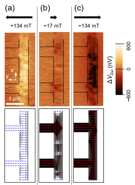
Fig. 2. The results of anomalous Nernst voltage mapping with (a) +134 mT, (b) −17 mT and (c) −134 mT.
We develop a simple method for magnetic imaging [3]. Our method only requires a conventional atomic force microscope with a high spatial resolution. Moreover, our technique can apply to antiferromagnetic Weyl semimetals that exhibit the anomalous Nernst effect.
References
- [1] S. Nakatsuji and R. Arita, Annu. Rev. Condens. Matter Phys. 13, 119 (2022).
- [2] A. Sakai et al., Nat. Phys. 14, 1119 (2018).
- [3] N. Budai, H. Isshiki, R. Uesugi, Z. Zhu, T. Higo, S. Nakatsuji, and Y. Otani, Appl. Phys. Lett. 122, (2023).