
Multiband Superconductivity in Strongly Hybridized 1T’-WTe2/NbSe2 Heterostructure
PI of Joint-use project: B. WeberHost lab: Hasegawa Group
Inducing superconductivity by proximity in materials with nontrivial band topology has become a method in the search for unconventional forms of superconducting pairing. At the one-dimensional (1D) edges of two-dimensional (2D) topological insulators the presence of non-Abelian parafermions has been predicted, which could have important applications in topological quantum computation. Here, we investigate heterostructures of the quantum spin Hall candidate 1T’-WTe2, grown by in situ van der Waals epitaxy on a superconductor 2H-NbSe2 by scanning tunneling spectroscopy down to 500 mK, which enables us to resolve the superconducting local density of states (LDOS) across the interface between the two materials.
Figure 1 shows scanning tunneling microscopy (STM) data of 1T’-WTe2/2H-NbSe2 heterostructures. In agreement with previous studies of WTe2 on bilayer graphene, we observe islands with disordered boundaries and sizes up to a few tens of nanometer in diameter that are polycrystalline on NbSe2 substrates. Lattice parameters estimated from FFT patterns of the STM images are a ~ a1 = 3.5 ± 0.2 Å, and b~2a2cos(30°) = 6.2 ± 0.3 Å, in good agreement with the lattice parameters of WTe2 (a = 3.48 Å and b = 6.28 Å) and NbSe2 (a1 = a2 = 3.45 Å). Local lattice matching implies a 5% compressive lattice strain along b, which has previously been shown to further stabilize the WTe2 bulk gap.
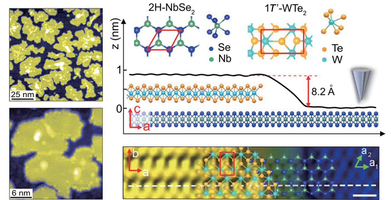
Fig. 1. (left panels) STM topography of monolayer 1T’-WTe2 islands grown on a single crystal of 2H-NbSe2 by van der Waals epitaxy. Upper right panel shows height profile corresponding to the dashed white line in the lower right panel, showing a monolayer height of 8.2 Å. The inset shows the respective 1T’-WTe2 and 2H-NbSe2 crystal structures. Atomic-resolution close-up of the 1T’-WTe2 edge, showing detail of the atomic alignment.
In Fig. 2, tunneling spectra taken on the monolayer WTe2 and the NbSe2 substrate at 500 mK are presented, demonstrating the clear signature of a superconducting energy gap in the 2D monolayer WTe2. The measured superconducting LDOS within a self-consistent multiband framework that considers a superconducting gap of each band and an interband Cooper-pair tunneling rate. It has been already known that the gap of NbSe2 is well described with a scheme of intrinsic two-band superconductor, and here we consider a third order parameter ΔWTe2, coupled to the two NbSe2 bands, assuming intrinsic ΔWTe2 = 0. Fits to both a two-band (NbSe2, red line) and a three-band (WTe2/NbSe2, blue line) model explain the data well (Fig. 2) and reproduce the known NbSe2 order parameters. Self-consistently obtained ΔWTe2 = (0.57 ± 0.02) meV, reflecting induced pairing, which suggests strong hybridization between the overlayer and substrate.
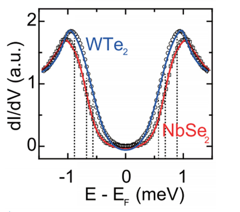
Fig. 2. tunneling spectra comparing the WTe2/NbSe2 spectrum with that measured on the bare NbSe2 substrate. Solid red and blue lines are fits to our two-band (NbSe2) and three-band (WTe2) models, respectively.
Our tight-binding calculations revealed that the strong hybridization in WTe2/NbSe2 heterostructure substantially weakens the topological edge state signature compared with WTe2/HOPG, which is only weakly hybridized. In spite of the suppressed edge states, however, we observed enhanced order parameter at the edge as shown in Fig. 3, where a spatial profile of the extracted order parameter ΔWTe2(x) based on the three-band superconductivity analysis is shown. The plot also shows spatial oscillations with a period of ~2 nm. Oscillations of comparable period are also observed in the order parameter extracted from a simple single-band BCS model. This suggests that these arise from Friedel-like oscillations in the local density of states due to scattering of 2D bulk states at the WTe2 edge. The exponential decaying 1D edge state, with decay length (1.1 ± 0.2) nm is comparable to the normal-state LDOS of the edge.
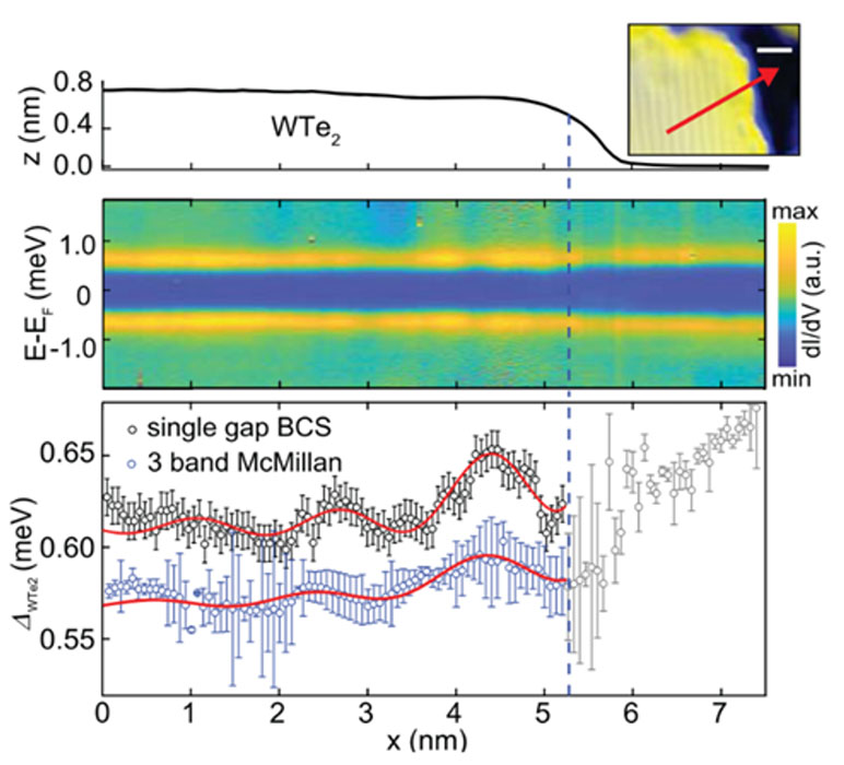
Fig. 3. (upper panel) STM-height profile measured across a clean edge of a WTe2 monolayer crystal. The inset shows the corresponding STM topograph indicating position and direction of the line profile (red arrow). (middle) A series of tunneling spectra measured T = 500 mK for points across the edge. (lower) Extracted spatial profile of the induced order parameter ΔWTe2(x) (blue), compared with a single-band BCS-Dynes model (black).
References
- [1] W. Tao et al., Phys. Rev. B 105, 094512 (2022).