
Nearly Room Temperature Ferromagnetism in a Pressure-Induced Correlated Metallic State of van der Waals Insulator CrGeTe3
Uwatoko Group
Discovery of two-dimensional (2D) magnetism in van der Waals (vdW) materials have unfurled diverse range of possibilities for development of novel spintronics, multiferroic and quantum computing devices using atomically thin materials [1]. Among the vast pool of vdW materials, CrGeTe3 and CrX3 (X = Cl, Br, I) are Mott insulators with a charge gap, thus facilitating suitable platforms to exploit both charge and spin degrees of freedom. At low temperature, these insulators share a common layered rhombohedral R3 -crystal structure held together by weak vdW forces along the c-axis. Each single layer consists of a honeycomb network of edge sharing octahedra formed by a central Cr atom bonded to six ligand atoms (Te or X), as illustrated in Fig. 1(a) for CrGeTe3.
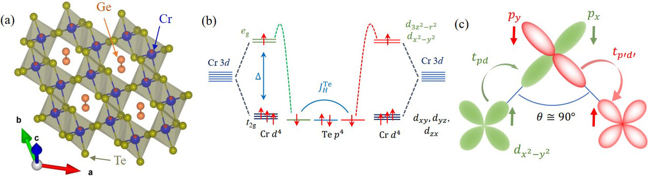
Fig. 1. (a) Single layer of CrGeTe3 illustrating the honeycomb network of edge sharing CrTe6 octahedra. In case of CrX3, the place of Ge-Ge dimers remains vacant. (b) Crystalline electric field splitting of Cr 3d orbitals into t2g - and eg -manifolds. ∆ is the energy difference between t2g- and eg levels. J
The crystalline field effect ensuing from this octahedra splits the Cr-3d orbitals into t2g - and eg-manifolds [Fig.1(b)]. The onsite Coulomb repulsion localizes the t2g-electrons driving the system into an insulating state significantly well above TC. Although, a direct antiferromagnetic exchange interaction exists between t2g-electrons, thermal fluctuation inherent to 2D suppress the long-range magnetic order. The spin orbit coupling (SOC) emanating through the covalent bond between ligand p and Cr-eg orbital generates the magnetocrystalline anisotropy energy to counteract the thermal fluctuation. Below TC, the superexchange interaction between Cr-eg electrons via two different ligand p-orbitals, as schematically portrayed in Fig.1(c), benefits from the distortion of CrTe6 octahedra and the Hund’s energy gain at the ligand Te (or X) site to stabilize the FM order. The correlation between t2g-electrons also move up the ligand p bands close to Fermi level, thus opening a band gap between the Cr d conduction band and the ligand p valence band indicating a charge transfer type Mott behaviour.
However, one drawback for the practical technological application is the low Curie temperature, TC, mostly below liquid nitrogen temperature. For exploitation of these attributes, it is essential to realize this novel FM state at or close to room temperature. Recently, TC of CrGeTe3 has been raised around 200 K either by intercalating large organic ions into single crystals [2] or using sophisticated process like electrochemical doping to field effect transistor devices [3]. Although, these results are promising, such filling control methods lead to strong charge inhomogeneity as well as structural and chemical defects, including creation of magnetic impurity, unfavourable for device application.
On the other hand, application of pressure is advantageous, which not only controls the bandwidth but also the spin exchange pathways via subtle modification of bond length and angle between atoms avoiding the complication of disorder. Here, for the first-time we show the evidence of nearly room temperature FM in CrGeTe3 bulk single crystals with application of pressure [4]. Using highly sensitive dc magnetic susceptibility and resistivity measurement under high quality hydrostatic pressure, we found that TC of CrGeTe3 exceeds 250 K above 9.1 GPa. In Fig. 2, we present the pressure-temperature phase diagram of CrGeTe3 which uncovers a rare example of bandwidth-controlled insulator-metal transition (IMT) in a vdW materials. Moreover, the remarkable absence of accompanied structural transition and spin crossover involving magnetic to non-magnetic states across IMT, clearly indicates the pressure driven changes of electronic property are purely electronic in origin. Furthermore, these findings show that electronic property of CrGeTe3 can be switched much more responsively using external perturbation, such as strain, doping compared to other vdW insulators.
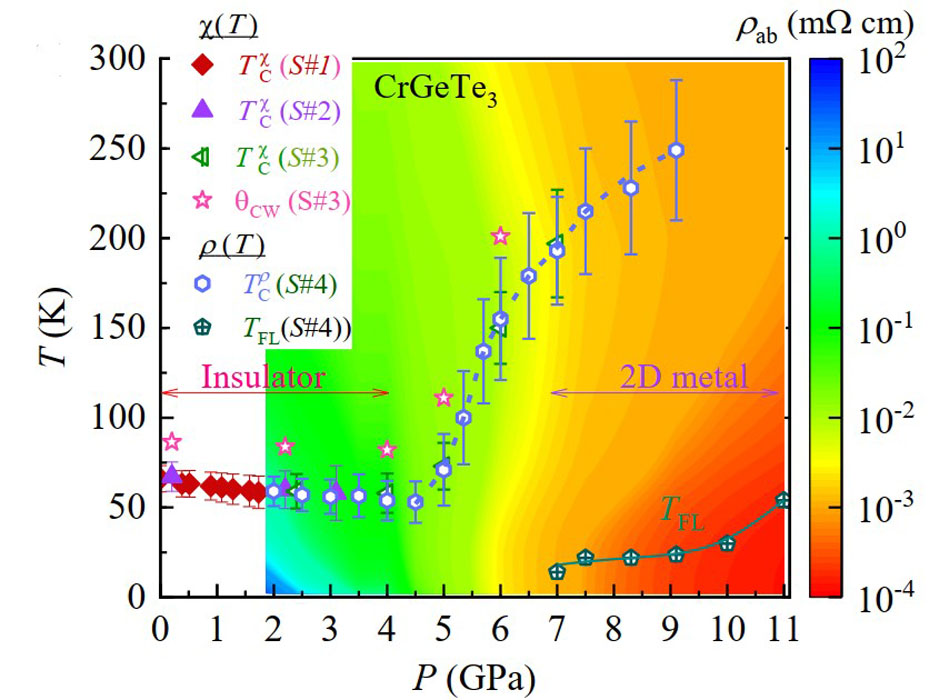
Fig. 2. Pressure temperature phase diagram of CrGeTe3. Color scale represents the magnitude of ρab. θCW and
References
- [1] C. Gong et al., Nature, 546, 265 (2017).
- [2] N. Wang et al., J. Am. Chem. Soc, 141, 17166 (2019).
- [3] I. A. Verzhbitskiy et al., Nat. Electron., 3, 460 (2020).
- [4] Dilip Bhoi, J. Gouchi, N. Hiraoka, Y. Zhang, N. Ogita, T. Hasegawa, K. Kitagawa, H. Takagi, K. H. Kim, and Y. Uwatoko, Phys. Rev. Lett. 127, 217203 (2021)