
Large Hall Signal due to Electrical Switching of an Antiferromagnetic Weyl Semimetal State
Nakatsuji, Otani, and Miwa Groups
The topologically protected properties in Weyl semimetals have been extensively studied in recent years. The Weyl points act as sources and drains of Berry curvature, leading to significant responses such as anomalous Hall effect (AHE) and anomalous Nernst effect (ANE) [1-3]. In nano-scale technology, such large topological responses may play a significant role in developing next-generation electronic devices.
Recently, the electrical manipulation of the topological state has been demonstrated in antiferromagnetic Weyl semimetal Mn3Sn [4]. Mn3Sn is a metallic antiferromagnet with the hexagonal D019 structure and ABAB-stacking of Mn kagome lattice along [0001]. The geometrical frustration leads to a 120-degree structure made of Mn magnetic moments with a negative vector chirality (Fig 1(a)). This non-collinear structure can be viewed as a ferroic order of a cluster magnetic octupole made of six neighboring Mn moments. The polarization of the magnetic octupole determines the distribution of Weyl points in momentum space and thus the polarity of AHE (Fig 1(b)). Figure. 1(c) shows the schematic image of the current switching in Mn3Sn/heavy metal heterostructures. Taking Mn3Sn/W as an example, with an applied electrical current in the multilayer, a spin current generated by the spin Hall effect in the W layer exerts the spin-orbit torque on the Mn3Sn spin texture, causing the switching of the polarization direction of the magnetic octupole. This manipulation of AHE enables us to store the information from the electrical signal, “0” or “1” state, into the magnetic octupole of Mn3Sn. Thus, Mn3Sn can work as a non-volatile memory, in which the information can be written and read by current. Moreover, the antiferromagnetic structure of Mn3Sn allows electronic devices with higher density and computing speed than those made of conventional ferromagnets [5]. For applications, it is essential to enhance the readout signal of the switching. This study demonstrates that the switching signal of Mn3Sn can grow dramatically by adjusting the crystal orientation and interface condition of the Mn3Sn/heavy metal structures. Moreover, by increasing the read current, the readout voltage may go well beyond 1 mV, a milestone for future memory technology.
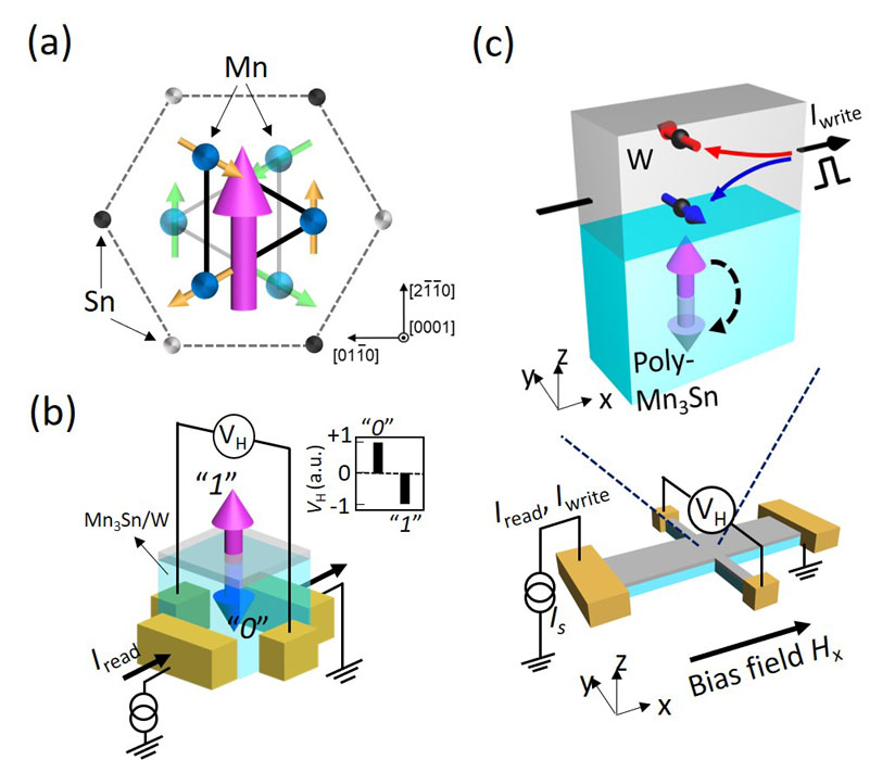
Fig. 1. (a) Crystal and spin structures of Mn3Sn. Blue and light blue spheres represent Mn atoms on the kagome bilayers, forming an octahedron. Black and gray spheres represent Sn atoms. The noncollinear spin structure consisting six Mn magnetic moments (yellow and green arrows) can be viewed as a ferroic ordering of an magnetic octupole (purple arrow). (b) Hall voltage measured in Mn3Sn/W devices. The sign of readout voltage is determined by the out-of-plane component in the polarization direction of the magnetic octupole of Mn3Sn (purple and blue arrows), namely, “0” or “1” state. (c) Bottom: Schematic image of Mn3Sn/heavy metal devices and the setup of electrodes. The samples are fabricated in 16 μm × 96 μm Hall bar structure with Au/Ti electrodes. Top: Schematic image of the current switching in Mn3Sn/W bilayer. An electrical current flowing in the W layer generates a spin current by the spin Hall effect of W. This spin current induces a spin-orbit torque in the Mn3Sn layer and switch the polarization direction of the magnetic octupole. Here, red and blue thin arrows represent the spin moments of the spin current. Purple and light purple thick arrows represent the polarization direction of the magnetic octupole.
To find the largest readout signal, we prepared four different multilayer stacks: (i) Ru(2)/Mn3Sn(40)/Pt(5), (ii) Mn3Sn(40)/Pt(5), (iii) Ru(2)/Mn3Sn(40)/W(5), and (iv) Mn3Sn(40)/W(5), all units in nm, deposited on a Si/SiO2 substrate. For the sample (i)-(iii), the stacks are annealed at 450 °C for 0.5 h after the fabrication of the Mn3Sn layer. The samples (iv) Mn3Sn(40)/W(5) is annealed at 450 °C for 0.5 h after the fabrication of the W layer. Using these thin films, a Hall bar structure (16 μm × 96 μm) is fabricated, with Ti/Au electrodes attached (Fig 1(c)). Figure. 2(a) shows the AHE signal in W devices with and without the Ru layer. By removing the Ru layer, the AHE becomes 1.6 times larger than that observed in devices with the Ru layer. Similar enhancement of the AHE also occurs in Pt devices. This enhancement comes from the crystal orientation change of Mn3Sn. The X-ray diffraction analysis shows that the kagome plane of Mn3Sn tends to align in-plane in the presence of the Ru underlayer. After removing the Ru layer, Mn3Sn layer becomes completely polycrystalline. The out-of-plane component of the magnetic octupole is more than one with the Ru layer, resulting in a larger AHE. Next, we investigated the electrical switching in W devices. In these experiments, both electrical current and bias field are applied along the longitudinal direction (x-direction) and the transverse Hall voltage VH is detected in the y-direction, as shown in Fig. 1(c). A strikingly large switching Hall voltage, ΔVHcurrent ~70 μV, is observed in Mn3Sn/W devices (Fig. 2(b)). This Hall signal is 3 times larger than that observed in the Ru/Mn3Sn/W devices, more pronounced than the 1.6 times difference of the AHE caused by removing the Ru layer. We attribute this enhancement in current switching to the different annealing process because only the Mn3Sn/W samples is once annealed after the W deposition. This additional annealing process may affect the interface condition. Finally, since the Hall voltage is proportional to the read current within a suitable temperature range, we tried to enhance the read current to maximize the readout signal (Fig. 2(c)). We found that the readout switching Hall voltage ΔVH can exceed 1 mV when applying 3 mA read current. This observed mV order Hall voltage is a significant advance in the electrical switching technology, and our results may pave the path for designing a new type of memory device using the robust topological properties of Weyl antiferromagnets.
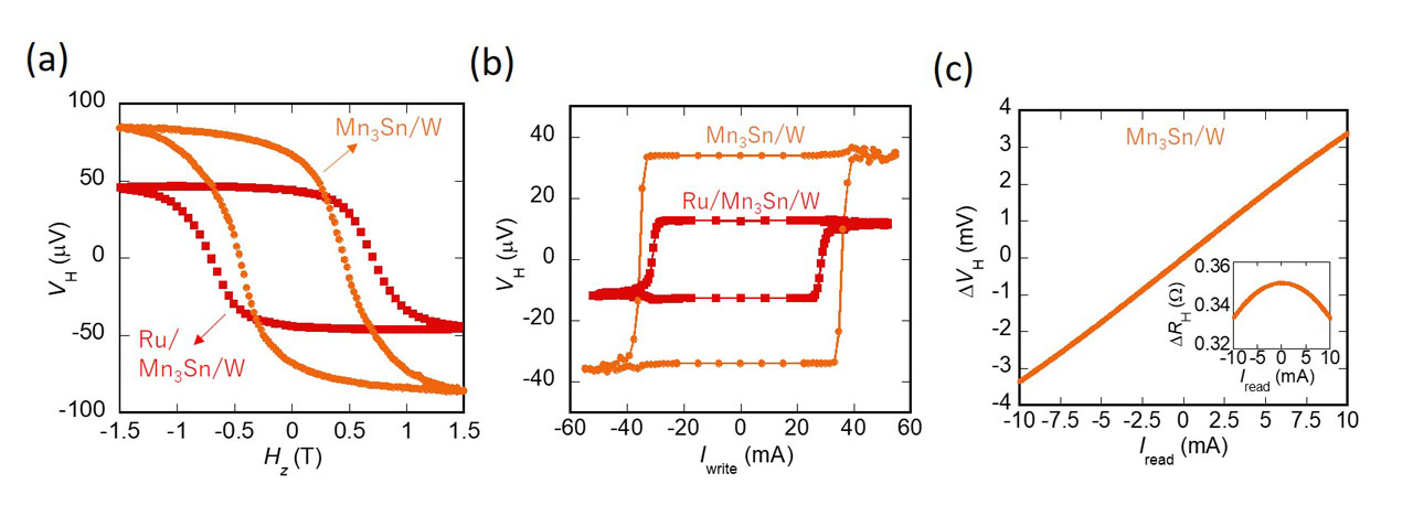
Fig. 2. (a) Hall voltage VH as a function of a perpendicular magnetic field Hz for Ru/Mn3Sn/W and Mn3Sn/W devices, respectively. (b) VH as a function of the write-current Iwrite under a bias field μ0Hx = 0.1 T applied along the electrical current direction for Ru/Mn3Sn/W and Mn3Sn/W devices, respectively. (c) Switching Hall voltage ΔVH as a function of the read current Iread in the Mn3Sn(40)/W(5) sample. Inset: Hall resistance ΔRH as a function of the read current Iread.
References
- [1] H. B. Nielsen and M. Ninomiya, Phys. Lett. B, 130, 389 (1983).
- [2] S. Nakatsuji, N. Kiyohara, and T. Higo, Nature, 527, 212 (2015).
- [3] M. Ikhlas, T. Tomita, T. Koretsune, M. Suzuki, D. Nishio-Hamane, R. Arita, Y. Otani, and S. Nakatsuji, Nat. Phys. 13, 1085 (2017).
- [4] H. Tsai, T. Higo, K. Kondou, T. Nomoto, A. Sakai, A. Kobayashi, T. Nakano, K. Yakushiji, R. Arita, S. Miwa, Y. Otani, and S. Nakatsuji, Nature 580, 608 (2020).
- [5] T. Jungwirth et al., Nat. Nanotechnol. 11, 231 (2016).