
Carrier Density Control in Oxide Quantum Wells
Lippmaa group
Two-dimensional carrier confinement in a quantum well at an oxide heterointerface offers new ways of controlling the transport behavior of oxide materials by applied external fields. Magnetic tunability has been attributed to Rashba-type spin-orbit coupling in an asymmetric electron distribution, the enhancement of spin-orbit coupling close to a filling-dependent Lifshitz transition, or a change in the effective disorder experienced by carriers when the quantum well width changes. Electric fields, on the other hand, can be used to change the quantum well filling, by accumulating or depleting carriers at an interface, or to modify the width of the electron distribution in the depth direction.
Oxide quantum wells are usually formed by growing a thin epitaxial LaAlO3 layer on SrTiO3, in which case the quantum well forms at the surface of the SrTiO3 substrate due to, at least in part, the change of lattice polarity at the interface. Instead of using the polar LaAlO3 layer, it is also possible to form quantum wells by depleting oxygen from the surface or by delta-doping SrTiO3 with a (La,Sr)Ox monolayer. All these techniques produce a metallic quantum well with qualitatively similar properties, but the LaOx delta-doping technique has several advantages in allowing a broad range of carrier densities to be explored. In contrast, the carrier number is essentially fixed by the polarity discontinuity at LaAlO3/SrTiO3 interfaces, while oxygen-deficient surfaces can only be maintained in ultra-high vacuum conditions.
In our recent work [1], we have studied the possibilities of constructing oxide quantum wells based on embedded (La,Sr)Ox layers in SrTiO3. The heterostructures were grown by Pulsed Laser Deposition on SrTiO3 single crystals as illustrated in Fig. 1. The carrier number in these heterostructures is controlled by two parameters: the number of La atoms in the delta-doping layer, and the thickness of a SrTiO3 capping layer. Since SrTiO3 surfaces exposed to air are strongly depleted, a space-charge layer forms in the cap layer and the thickness of the capping layer can be used to partially deplete the carriers in from the quantum well. Almost complete carrier depletion occurs when the capping layer thickness drops below 4 nm (10 unit cells). Above 10 nm capping thickness, surface depletion no longer affects the carrier density in the quantum well and the carrier density is set by the number of La atoms in the delta-doping layer. The built-in carrier density in the quantum well is thus set by two layer thickness parameters that are easy to control with precision in the growth process. When the heterostructures are formed into gated field-effect transistors, additional fine-tuning of the carrier density over a narrow range is possible by applying a suitable gate voltage. The electrostatically-gated heterostructure devices are thus particularly well suited for studying filling-dependent Lifshitz transitions, i.e. varying the Fermi energy in the quantum well across the Ti 3d conduction band dxz,yz - dxy level crossing.
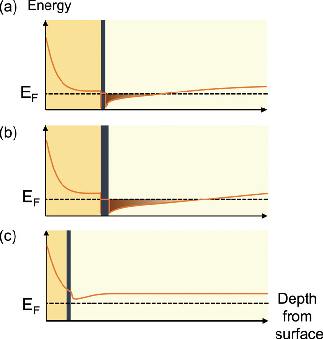
Fig. 1. Formation of a quantum well in SrTiO3 around a LaTiO3 delta doping layer. Due to surface depletion, carriers are depleted from the quantum well if the distance is small (c). Saturated metallic behavior is obtained only for capping layers thicker than 10 nm (a).
The effects of the doping and capping layer thicknesses on the transport behavior of the heterostructures are shown in Fig. 2. When a thick capping layer is used and the surface depletion effect can be ignored, metallic conductivity is obtained from the LaOx layer coverage exceeds about 0.3 monolayers and a gradual reduction of the sheet resistance is observed as the La coverage is increased. For a single unit cell of LaTiO3, the quantum well carrier density was on the order of 1013 cm-2. In all cases, however, the Hall resistance was nonlinear, indicating that a significant depth distribution of carriers exists. Approximately 1/4 of the carriers are distributed to a distance of 10 nm or more from the interface. These ‘deep’ carriers do not suffer from interfacial scattering and reach a mobility of over 104 cm2/Vs at 4K.
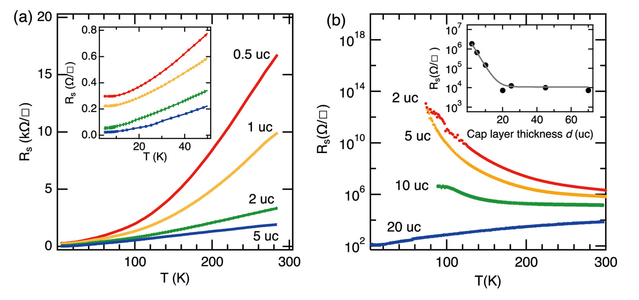
Fig. 2. Variation of the sheet resistance of SrTiO3/LaTiO3/SrTiO3 heterostructures with the LaTiO3 delta-doping layer thickness (a) and SrTiO3 capping layer thickness (b). Layer thicknesses are given in unit cells (4Å).
The built-in carrier concentration can be further adjusted by changing the cap layer thickness, as shown in Fig. 2b. As the cap layer thickness is reduced to 10 unit cells or less, the heterostructures become semiconducting and finally insulating. These experiments show that it is possible to tune the carrier density continuously close to the lowest densities where metallic conductivity can be sustained.
References
- [1] J. N. Lee, X. Hou, R. Takahashi, and M. Lippmaa, Appl. Phys. Lett. 116, 171601 (2020).