
Cyclotron Resonance in Near Surface of InAs Quantum Well
G. A. Khodaparast, B. A. Magill, and Y. H. Matsuda
Electronic states of semiconductor nanostructure near surface has been attracting much attention in terms of controlling quantum effects that can emerge through correlation with a superconductor. Josephson junctions made from Al-InAs have been used to create tunable superconducting qubits [1]. The key feature of the superconductor (Al) and semiconductor (InAs) nanostructure is that the two-dimensional gas (2DEG) is confined near the surface, in close proximity to the superconductor.
Although the electronic state of a bulk InAs is well understood, it is expected that the quantum confinement effect modifies the electronic state. Moreover, a narrow gap semiconductor exhibits small effective mass and large g factor, and the non-parabolicity of the band due to the confinement affects these fundamental parameters. Investigation of the electronic state of the 2DEG in InAs quantum well is essential for development of the novel semiconductor-superconductor device. In the present study, the cyclotron resonance (CR) of an InAs quantum well has been investigated. Clear spin-split cyclotron resonance has been observed and the effective mass and the g factor are deduced as a function of magnetic field.
The CR experiment was performed with the single-turn coil (STC) at the ISSP for magnetic field generation and an infrared CO2 gas laser as the light source. The wavelengths used were 9.22, 10.48, and 10.6 μm. The laser light shines the sample and the transmitted light intensity was measured as a function of time during a pulse of a magnetic field (B) generated by the STC. A high speed HgCdTe PIN photo diode was used for detection of the light signal. The samples were grown on a semi-insulating InP (100) substrate, using a molecular beam epitaxy system. The InxAl1−xAs buffer is grown at low temperature to help mitigate formation of dislocations originating from the lattice mismatch between the InP substrate and higher levels of the heterostructure [2]. The indium content of InxAl1−xAs is step-graded from x = 0.52 to 0.81. Next, a delta-doped Si layer of ~ 7.5 × 1011 cm−2 density is placed here followed by 6 nm of In0.81Al0.19As. The quantum well is grown next, consisting of a 4 nm thick layer of In0.81Ga0.19As layer, a 4 nm thick layer of InAs, and finally a 10 nm thick top layer of In0.81Ga0.19As.
Figure 1 shows the CR spectra at 300 and 20 K. In the upper panel, the CR peaks around 40 T indicated by solid allows are interpreted as the spin-split resonances : They are the inter-Landau level transitions between n = 0 and n = 1 with different spin polarization, where n is the Landau level index. Another CR peak at around 55 T is, on the other hand, due to the transition between n =1 and n = 2 levels. When the temperature is lowered to 20 K, only one of the spin-split CR peaks is observed, which can be explained in terms of the population of carriers. They populate only in the lowest level at a low temperature. Remaining 55-T CR peak confirm that this resonance is due to non-equilibrium distributed carriers.
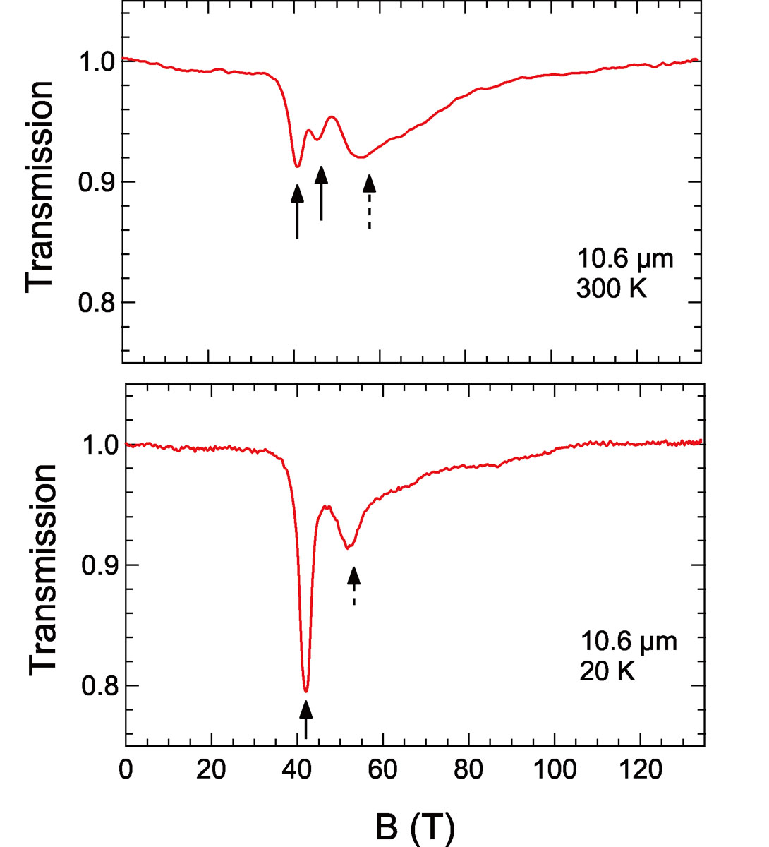
Fig. 1. Cyclotron resonance (CR) in the InAs quantum well. The upper panel shows the resonance spectrum at 300 K. The two solid arrows suggest the spin-split CR. The broad CR indicated by the dashed arrow is due to the inter-Landau level transition between n = 1 and n = 2. The lower panel shows the CR at 20 K. Observation of only single peak near 40 T indicates effect of the thermal population of carriers. Since the CR around 55 T is considered to be due to the non-equilibrium of electrons, it remains at a low temperature.
The effective mass of electrons (m*) is directly deduced from the peak position Bc. The left-panel of Fig. 2 shows the magnetic field dependence of m*. It is found that they are considerably larger than the band-edge effective mass of a bulk InAs 0.023m0, where m0 is the mass of a free electron. The large effective mass is due to the quantum confinement effect and the cyclotron energy. The enhancement of m* with increasing magnetic field is interpreted as a result of the non-parabolicity of the band due to the cyclotron energy. The g factor can also be obtained by comparison between the CR peak position and the calculated inter-Landau level energies. It has been found that the g factor becomes small with increasing cyclotron energy. The g factor of a bulk InAs is known to be -14.
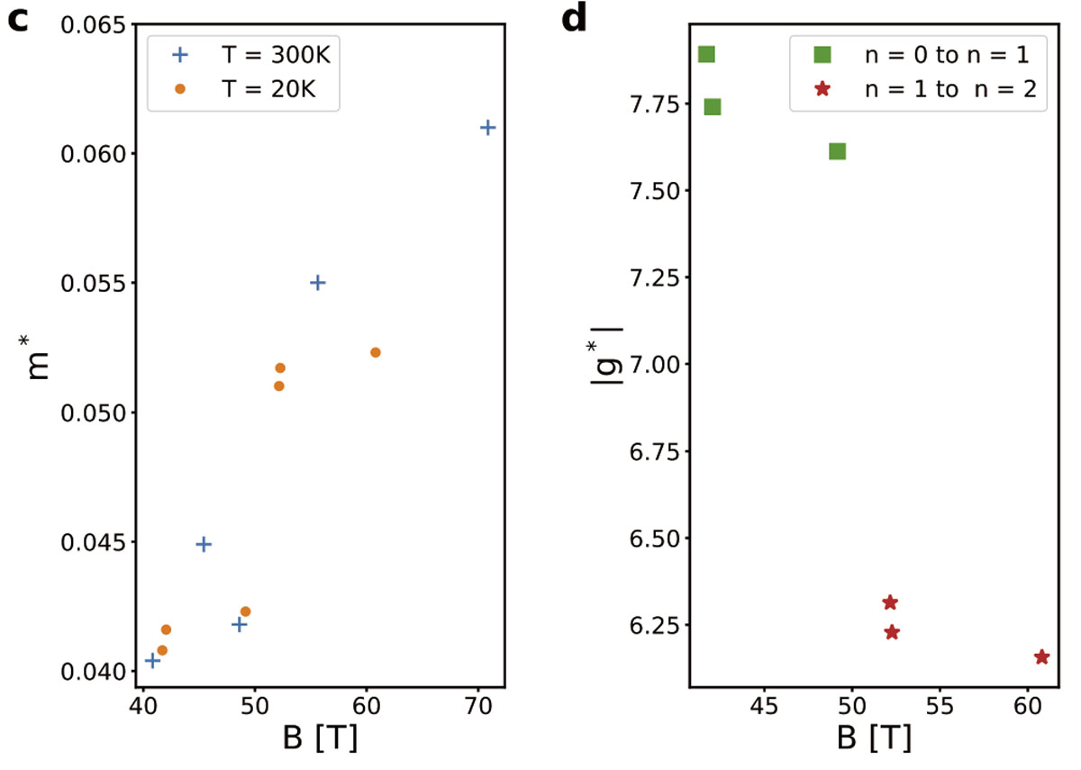
Fig. 2. Left-side panel: The obtained effective mass of electrons. The rather large field variation indicates the strong non-parabolicity of the energy band. The right-side panel: The g-factor deduced from the experiment and numerical analysis. It is clear that g-factor is also affected by the non-parabolicity.
The magnetic field dependences of the m* and g leads us to the values at zero magnetic fields and they are found to be 0.027m0 and -12, respectively [3]. Determination of these quantum parameters will significantly contribute development of the novel Josephson-junction devices.
References
- [1] T. W. Larsen, K. D. Petersson, F. Kuemmeth, T. S. Jespersen, P. Krogstrup, J. Nygard, and C. M. Marcus, Phys. Rev. Lett. 115, 127001 (2015).
- [2] J. Shabani, S. Das Sarma, and C. J. Palmstrøm, Phys. Rev. B 90, 161303 (2014).
- [3] J. Yuana, M. Hatefipoura, B. A. Magillb, W. Mayera, M. C. Dartiailha, K. Sardashtia, K. S. Wickramasinghea, G. A. Khodaparastb, Y. H. Matsuda, Y. Kohama, Z. Yang, S. Thapac, C. J. Stantonc, and J. Shabania, Phys, Rev. B 101, 205310 (2020).