
Electronic Structures of 4º-Twisted Bilayer Graphene Fabricated in a Vacuum
S. Tanaka and F. Komori
Twisted bilayer graphene (TBG) is a stacked two graphene sheets with mutually in-plane rotation, and exhibits electronic states different from those observed in a typical bilayer graphene with Bernal stacking. Its Fermi velocity in the vicinity of the Dirac point strongly depends on the twist-angle θ below 10º [1], and vanishes around a magic angle of θ ~ 1.1º [2]. At this magic angle, a flat band with extremely sharp density of states is thus realized, and its electronic properties have attracted much attention. TBG is usually prepared by stacking mechanically-exfoliated graphene sheets in air, and thus it is difficult to prepare a millimeter-scale samples with clean interface between the sheets for using standard surface analysis techniques such as various diffraction methods and high-resolution photoemission spectroscopy. To prepare wide TBG’s with clean interface, we have developed a new method of directly bonding clean graphene sheets in a vacuum without any chemical adhesion and transmission media. For this purpose, we use monolayer graphene that can be easily exfoliated from the SiC substrate [3]. The band structure observed by angle resolved photoemission spectroscopy (ARPES) exhibits changes of the electronic states due to the interlayer interaction [1].
Graphene sheets are made on a 4H-SiC (0001) substrate by chemical vapor deposition (CVD) using ethylene. A buffer layer with a 3 × 3 periodicity is formed at the interface between the graphene and substrate, and allows us to exfoliate the graphene layer easily. It is noted that graphene on the thermally decomposed 6√3 × 6√3 -R30º buffer layer (6R3) coexists. The TBG samples are prepared at 200 ºC in a vacuum by pressing together for 1 hour and detached at the same temperature. The samples were then evaluated by optical microscope, μ-Raman spectroscopy, low energy electron diffraction (LEED), scanning tunneling microscopy (STM) and ARPES. Sub-millimeter areas with TBG were confirmed on the substrate.
Observed LEED and STM images of a 4º-rotated TBG are shown in Fig. 1. Two sets of 6-fold bright graphene spots with surrounding satellite spots are seen in Fig. 1(a), and correspond to lower-layer (gCVD) and upper-layer transferred (gtr) graphene. In the STM image, a moiré pattern due to the twisted layers is observed with the graphene lattice. The twist angle θ is estimated from the satellite-spot periodicity and the moiré image. Graphene band structures measured by ARPES at 300 K using 52 eV synchrotron light (KEK-PF, BL13) are shown in Fig. 2. Two graphene Dirac cones appear at Fermi energy (EF) as in Fig. 2(a). The band structure shown in Fig. 2(b) indicates the both graphene layers are p-doped. The cone at negative ky originates from the transferred graphene on the 3 × 3 substrate. In addition, an n-doped Dirac band is seen in Fig. 2(b), which originates from the transferred graphene on the 6R3 substrate. Energy gap of the bands due to the interlayer interaction is found at ky = 0 in the same figure. The Dirac band shown in Fig. 2(b, right) has a kind structure at 0.2 eV.
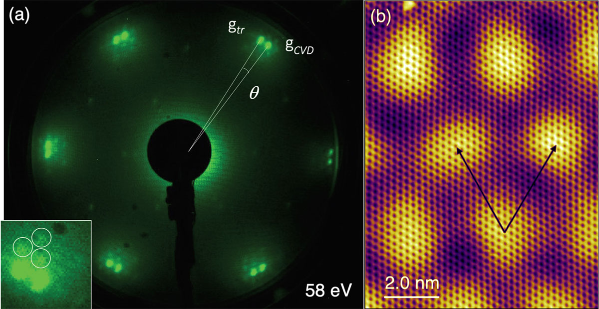
Fig. 1. (a) LEED pattern at the area with TBG. Bright 12 spots are identified as two sets of 6-fold symmetric graphene diffraction spots from the lower (gCVD) and upper (gtr ) layers. Inset shows the magnified image of the graphene diffraction including satellite spots (circles) due to the moiré structure. (b) STM image taken at the TBG area, showing graphene atomic image and moiré lattices. Moiré unit cell of the lattice is indicated by arrows. The image was taken at the sample bias voltage 0.8 V and tunneling current 0.5 nA at 80 K [3].
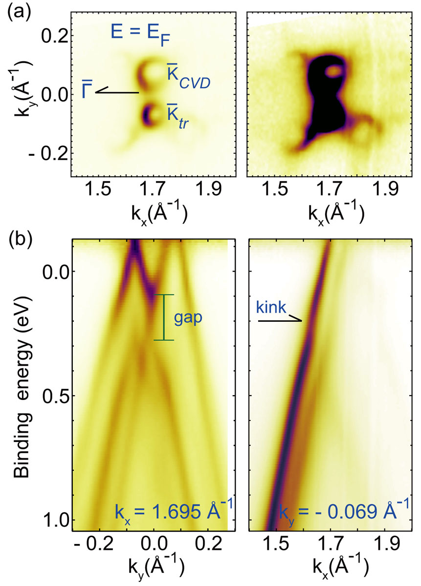
Fig. 2. ARPES constant energy and band dispersion maps. The kx axis is on the line between the middle of the two K points of the graphene layers (KCVD, Ktr) and Γ point. (a) Constant energy maps at EF without (left) and with (right) image enhancement. Replica bands are seen at this energy as in left. (b) Band dispersions along ky axis at kx = 1.695 Å-1 (left) and along kx axis at ky = - 0.069 Å-1 (right). Here, the ARPES intensity is normalized by the Fermi-Dirac distribution function at 300 K. Two Dirac bands of the transferred graphene are seen at negative ky in the left figure [3].
References
- [1] J. M. B. Lopes dos Santos et al., Phys. Rev. Lett. 99, 256802 (2007).
- [2] R. Bistritzer, and A.H. MacDonald, Proc. Natl. Acad. Sci. U. S. A. 108, 12233 (2011).
- [3] H. Imamura et al., Appl. Phys. Express 13, 075004 (2020).