
Patterning of Topological Insulator on Thin Film
H. Mine, J. Haruyama and T. Nakamura
Because topological insulators (TIs) have their conducting channels at the sample edges, shapes of them play crucial roles in device applications. Hence it can be a very convenient tool if we can “draw” spatial patterns of TI just like drawing a picture. Members of two-dimensional (2D) transition metal dichalcogenides (TMDCs) have been predicted and experimentally confirmed as a new class of 2D TI materials though the edge conduction is fragile in most cases. Here, we realize the controlled patterning of a TI phase embedded in an insulating phase of thin molybdenum-disulfide (MoS2) by laser beam irradiation.
MoS2 is known to have various metastable lattice structures according to the freedom in the stacking angle of the chalcogen layer. In so called H-phase, the chalcogens form triangle poles or trigonal prism. In single crystal, two-layers form a unit and called 2H phase. This is semiconducting.
In so called T-phase, the two-triangles are in the twisted relation. The stacking unit is single and called 1T phase. This is metallic. These two are the representative phases but there are many other metastable phases.
An interesting is the one called 1T’ phase, which is somewhat intermediate between these two. In this 1T’ phase, for example this upper chalcogen atoms shift in this way and stop at some intermediate position. Some theories predict this 1T’ phase should be a topological phase. So if we can cause local phase transition between these three, we can make up desired circuits with semiconductors, metals and topological insulators. We showed that 1T’ phase can be actually created in 2H MoS2 and also it works as a TI [1].
In order to obtain 1T’, we used the excitation by Ar laser beam of energy 2.5 eV and simply drew some patterns on 2H MoS2. From an atomic force microscope topography, it turned out that the irradiated region is a bit thinner than the surrounding region. This is probably due to some evaporation of atoms and the phase transition is not due to the direct energy transfer from photon to lattice but some heating effect causes the transition. The appearance of 1T’ phase was confirmed in the Raman and the XPS spectra as shown in Fig. 1 (a) and (b).
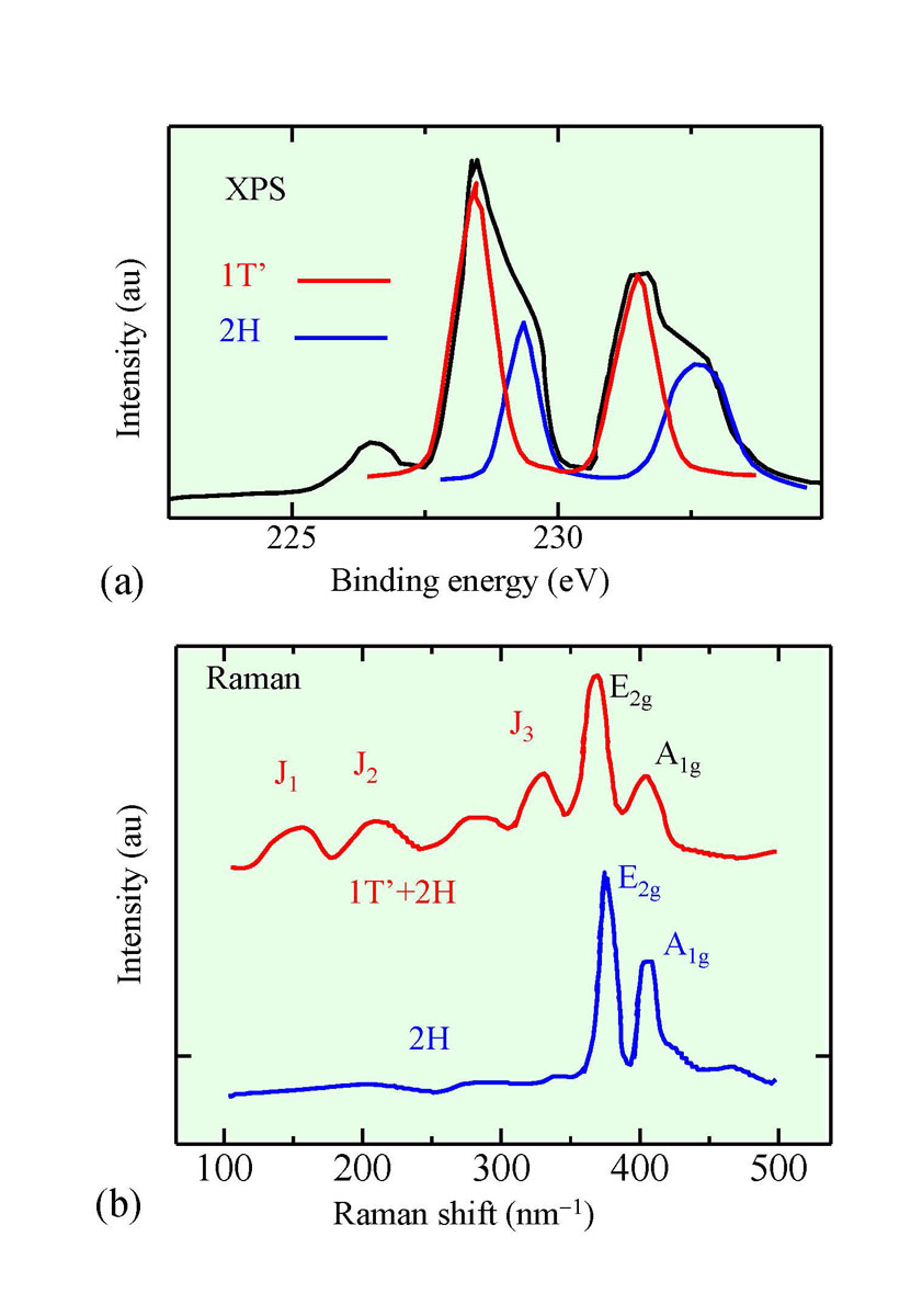
Fig. 1. (a) X-ray photoelectron spectroscopy taken at a laser-irradiated region (black line). Red and blue lines are those expected for 1T’ and 2H phases respectively.(b) Raman shift spectra. Blue: 2H phase before laser irradiation. Red: mixture of 1T’ phase and 2H phase after irradiation.
The pattern of 1T’ phase we used for the measurement of edge channel conduction is a simple H-shape as illustrated in the inset of Fig. 2. The size is about 2 μm, which is comparatively large compared with ordinary reported coherence length of edge conductions in TIs. The flake of MoS2 was placed on a metallic doped Si substrate covered with SiO2, hence we can tune the position of Fermi energy in MoS2 wtih the back gate voltage. Figure 2 shows the resistance of H-shaped sample in the measurement geometry drawn in the inset, as a function of the back gate voltage. The resistance R took a peak structure around at R = Rq/2 = h/2e2 = 12.6 kΩ. This is the value calculated for ideal helical edge states and clearly tells that the patterned 1T’ was working as a TI. The resistance quantization persisted surprisingly up to room temperature manifesting an opening of large spin-orbit energy gap. The gap closing around the sample edges was also confirmed with a scanning tunneling spectroscopy.
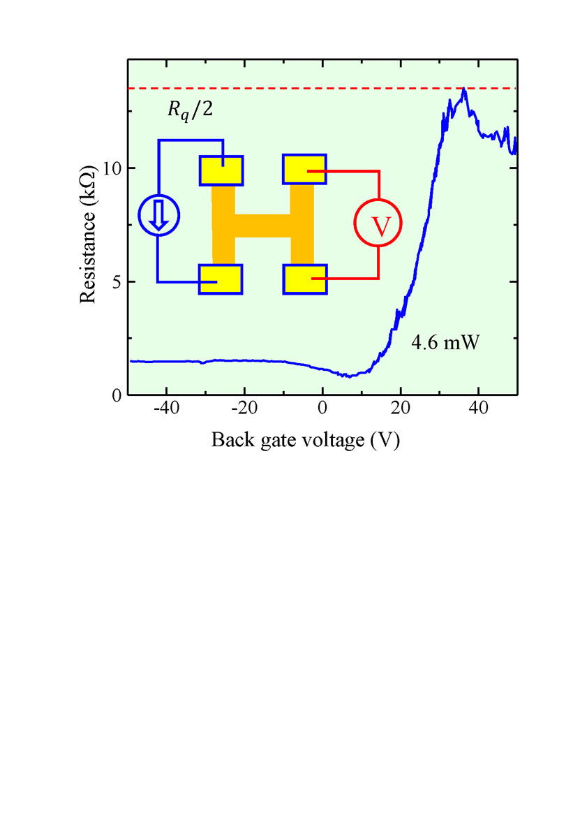
Fig. 2. Resistance of laser irradiated pattern on MoS2 as a function of back gate voltage. In the inset we illustrate the setup of resistance measurement.
References
- [1] H. Mine, A. Kobayashi, T. Nakamura, T. Inoue, S. Pakdel, D. Marian, E. Gonzalez-Marin, S. Maruyama, S. Katsumoto, A. Fortunelli, J. J. Palacios, and J. Haruyama, Phys. Rev. Lett. 123, 146803 (2019).