
Surface-State Coulomb Repulsion Accelerates a Metal-Insulator Transition in Topological Semimetal Nanofilms
I. Matsuda, Sugino, and Komori Groups
By reducing the size of materials in the microscopic scale, the electronic states are governed by the rules of quantum mechanics and the various quantities, such as energy levels, take discrete values (the quantum size effect, QSE). Thus, there can be a case that gapless metal films become insulating at the nanoscale. Such a QSE-induced transition into an insulating phase in semimetallic nanofilms was predicted more than half a century ago on bismuth (Bi) films [1]. Despite the researches of spectroscopy and transport experiments, the previous results have remained contradictions, indicating an interesting mechanism behind.
In the present research, we revealed an unexpected mechanism of the transition in Bi by combining of high-resolution measurements of angle-resolved photoemission spectroscopy (ARPES) on high-quality films and the density-functional theory (DFT) calculations [2]. Figure 1 (a) shows peak-enhanced ARPES images resolving all quantized bulk bands and surface bands. One can see that the top quantized levels are clearly shifting below the Fermi level with decreasing thickness. This is the first direct observation of the QSE-induced transition into an insulating phase in Bi films.
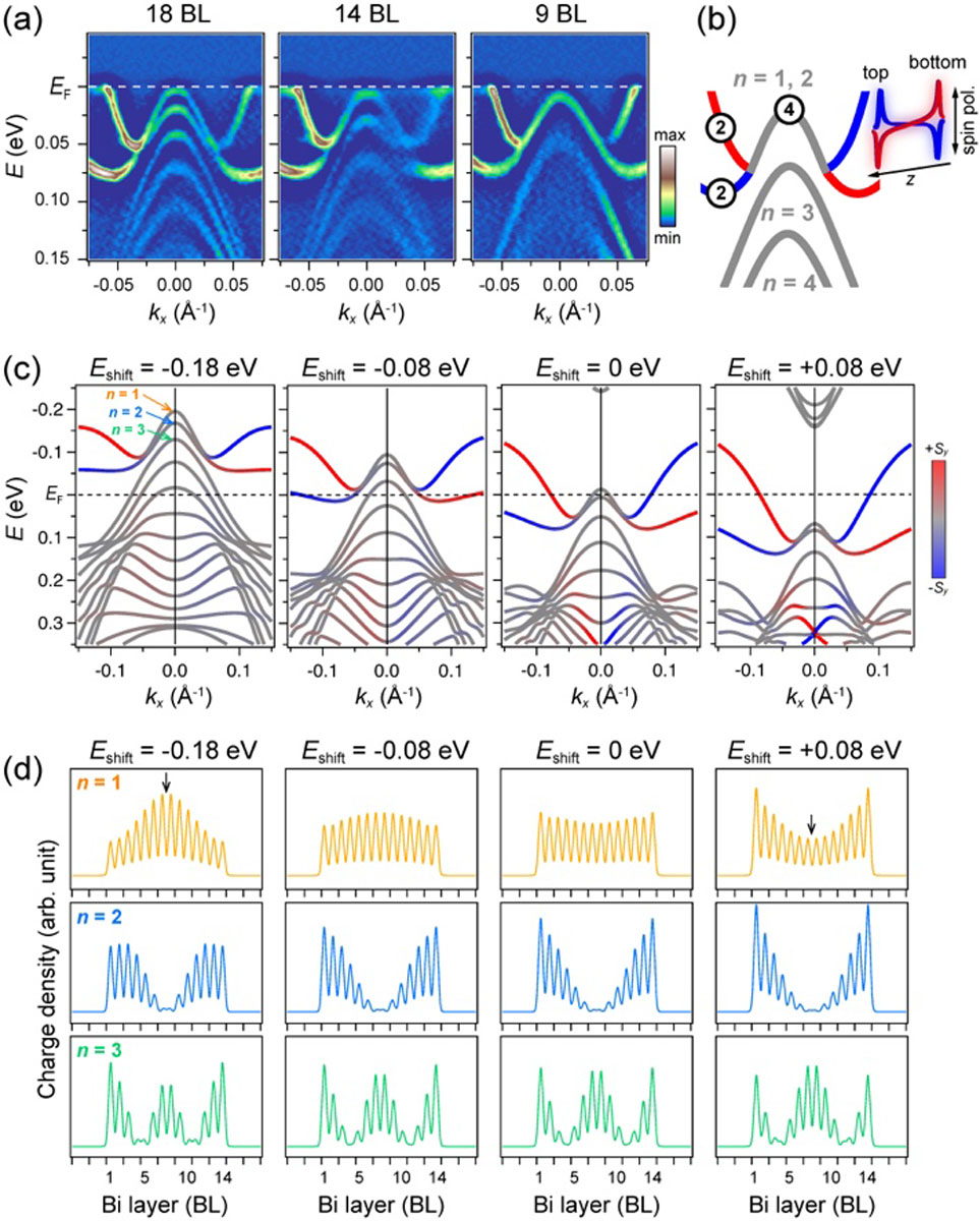
Fig. 1. (a) Peak-enhanced ARPES images measured on atomically thin Bi films. 1 bilayer (BL) of Bi corresponds to 3.9 Å. (b) Schematic of unusual band connections. The number indicates degeneracy of each band. (c) DFT band structures calculated on a 14 BL Bi slab with energy shifts manually induced. (d) Wave function characters calculated for n = 1, 2, 3 quantized states.
The high-resolution ARPES observation reveals an unusual signature: both of two surface bands connect to the top quantized bulk band. Because of the presence of surface states at the top and bottom of a film, these surface bands are doubly degenerate. Thus, this band connection readily means that the top quantized level must be quadruply degenerate. Although this breakup of conventional quantization rule was totally unexpected, our first-principles calculations reproduced the behavior. In Fig. 1(c) shows band structures that are intentionally shifted via modulation of lattice parameters. In the leftmost panel, quantized energy levels are regularly ordered, and n = 1, 2, 3 states possess wave function characters expected for ones confined in an ideal quantum well. From the leftmost to the rightmost panels, the separation between n = 1 and 2 levels is gradually reduced, and the wave function characters divert from the ideal cases and get localized near surfaces.
What is the essential mechanism for the unexpected level degeneracy and the bulk-to-surface transformation of quantized wave functions? In the DFT framework, an effective one-body potential and a total charge density are determined by a self-consistent cycle reflecting Coulomb interaction. From left to right in Fig. 1(c), the occupation of the surface bands increases and their relative contributions to the total charge density increase.
This tendency makes Coulomb repulsion among electrons compress the total charge density toward the film center. In the one-body picture of the DFT framework, a potential barrier around the film center is induced by this compressed total charge, which creates a double-well potential, as illustrated in Fig. 2(a). Such a double-well potential supports degenerate ground states whose wave functions are localized in both wells with opposite parity, which explains observations above. Furthermore, experimental thickness dependence of quantized levels was excellently reproduced by a numerical simulation using a single-well potential which gradually deforms into a double well (Fig. 2(b)).
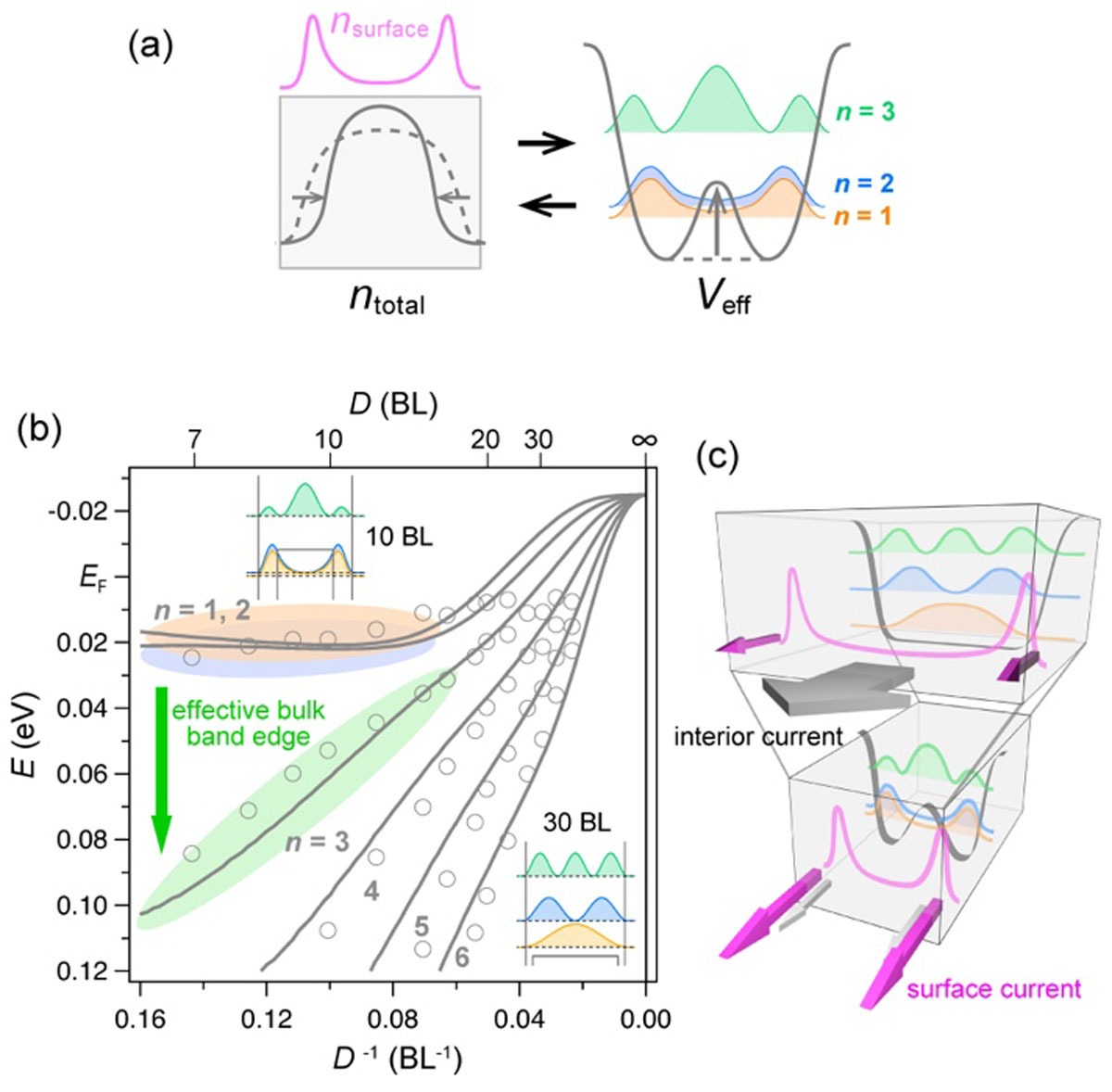
Fig. 2. (a) Schematic of a self-consistent cycle for a total charge density and an effective confinement potential. (b) Comparison of experimental thickness dependence of quantized levels (markers) and a numerical simulation (solid lines). The inset depicts wave function characters obtained in the simulation. (c) Schematics of the new class of size effects driven by increased Coulomb repulsion from surface states.
This unprecedented picture naturally reconciles the strange contradiction observed in previous studies: even if the top quantized levels can cross the Fermi level, the states effectively behave as surface-conducting states, and the film interior is insulating as observed in transport experiments, as shown in Fig. 2(c). Thus, we established the complete picture of the half-century problem in Bi, which demonstrates a new class of size effects driven by increased Coulomb repulsion from surface states.
References
- [1] V. B. Sandomirskii, Quantum size effect in a semimetal film. Soviet Physics JETP 25, 101 (1967).
- [2] S. Ito, M. Arita, J. Haruyama, B. Feng, W.-C. Chen, H. Namatame, M. Taniguchi, C.-M. Cheng, G. Bian, S.-J. Tang, T.-C. Chiang, O. Sugino, F. Komori, and I. Matsuda, Science Advances 6, eaaz5015 (2020).