
Nanoscale Potential Mapping: Direct Visualization of Electrical Resistance at Single Surface Steps
Hasegawa Group
Atomically-thin two dimensional electron systems (2DES) have been one of the hot topics because of their unique properties originating from the low dimensionality and reduced symmetry. Among them 2DES by metallic surface states, which are formed by a few monolayer (ML) deposition of metallic elements on semiconducting substrates, have a unique status. Because of the thermal stability through the surface reconstruction, self-organized high-quality periodical structures can be formed in macroscopic dimensions. Basic properties such as atomic structure and electronic states can be well characterized by standard surface science techniques including scanning tunneling microscopy (STM). Recent discovery of superconductivity in surface 2DES attracted further attentions.
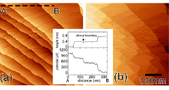
Fig. 1. STM (a) and electrochemical potential (b) images taken simultaneously on the Si(111)7×7 surface. (inset) cross-sectional plots of topographic height and potential taken along the dashed line drawn in (a).
Net and local misorientations of the substrate from a nominal plane results in the formation of steps on it. Superstructure due to the surface reconstruction inherently forms boundaries that separate domains whose periodical phases are different from each other. Both of the one-dimensional line defects disrupt the periodicity of the surface atomic arrangement and therefore work as a barrier for the electrons across them. In order to investigate the role of the line defects in electrical transport, we measured the nanometer-scale spatial distribution of local electrochemical potential of an archetypical metallic surface states; the 7×7 structure of Si(111) substrates, using an STM-based technique called scanning tunneling potentiometry (STP) [1]. Using STP, we found potential drops clearly at step edges and phase boundaries of the 2D metallic surface, demonstrating the presence of significant electrical resistance there.
Figure 1 shows STM and electrochemical potential images taken simultaneously on the 7×7 surface under the net current flow from the left to the right. A single-height (0.31 nm) steps are observed running from the upper left to the lower right in the topographic image (Fig. 1(a)). In the corresponding potential image (Fig. 1(b)), potential drops are found at the step edges, as more quantitatively presented in the inset cross-sectional plots, which was taken along the dashed A-B line in Fig. 1(a).
The steps are, however, not the only defects that disrupts the electron transport on the surface. In the potential mapping, which exhibits a ladder-like pattern, one notices several potential drops in narrow terraces separated by the steps. The potential drop due to the rungs of the ladders is more clearly displayed in a cross-sectional profile shown in the inset. The rungs correspond to boundaries that separate domains of the 7×7 reconstructed structures whose phases do not match. The potential images indicate that the phase boundaries also have electrical resistance.
From the obtained potential images and their cross-sectional plots, we can quantitatively analyze the conductivity through an individual step and phase boundary. Since the absolute value of the current density is unknown, we cannot measure the terrace, step, or phase boundary conductivity directly. But, their ratio can be estimated precisely. Since in our measurement we used low-doped substrates, the electrical conductance through the substrate is quite small. The poorly conductive substrate safely eliminates the problem of the bulk contributions in our measurements.
We estimated the conductivity ratio of the step to the terrace σs/σt is 3.1±1 /μm. The ratio means that the resistance of a single step corresponds to that the 340 nm-width terrace of the 7×7 structure. This also implies that the contribution of the steps to the net resistance dominates when the tilting angle of the surface exceeds 0.06°, which is much smaller than the tolerance of the miscut angle (~0.16°) for commercial wafers. The macroscopic net resistance through the 7×7 surface states, which include both those of terraces and steps, is therefore basically determined by the step density and the misoriented angle of the substrate.
The phase boundary is found more conductive than the step: the conductivity ratio of a single phase boundary to terrace σph/σt is 16.4 ± 10 /μm. The density and distribution of phase domains of the 7×7 structure are closely related with nucleation process of the 7×7 structure from disordered 1×1 during the cooling of the sample after the annealing to get rid of the surface oxide layer and to form the clean 7×7 structure. The macroscopic surface conductivity, therefore, also depends on the sample preparation method; e.g. how the sample was slowly cooled after the annealing.
In fact, the electrical conductivity of the surface has been characterized in various methods including microscopic 4-probe methods, but the measured conductivity have been widely dispersed. Our results indicate that the macroscopic net conductivity are mostly determined by the density of steps and domain boundary, thus depending strongly on the misorientation of the sample and its preparation. The present study also demonstrates the importance of characterizing microscopic conductance to elucidate the intrinsic transport properties of the system.
References
- [1] M. Hamada and Y. Hasegawa, Jpn. J. Appl. Phys. 51 125202 (2012).
- [2] M. Hamada and Y. Hasegawa, Phys. Rev. B 99, 125402 1 (2019).