
In-Plane Spin Filtering in a Resonant Diode with Double Quantum Well
Katsumoto Group
A quantum resonant diode is a device that filters the electron momentum perpendicular to the quantum well. Combined with the energy conservation, this restricts the electrons which can tunnel through the device into a circle on the Fermi surface in the source. The momentum selection may lead to spin selection due to spin-momentum locking via strong spin-orbit interaction (SOI). This can be achieved, for example, in a series connection of two quantum wells with opposite sign Rashba SOI coupling constants to each other [1]. However this device does not have practical meaning because Rashba-type SOI does not have in-plane anisotropy and without in-plane selection of momentum, the device does not work as a spin-filter. Now, if Dresselhaus-type SOI co-exists, the in-plane symmetry of the system lowers and the device can have bi-directional spin-filtering effect.
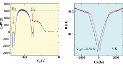
Fig. 1. Left: Differential resistance of an InGaAs double quantum well resonant diode as a function of source-drain negative bias voltage. E1 and E2 correspond to the resonant energy levels. Right: Hysteretic in-plane magnetoresistance appeared above the resonant level E1. The field direction is along [110]. Blue and red lines correspond to down and up field sweeps respectively.
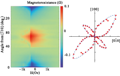
Fig. 2. Left: Color level plot of the magnetoresistance as a function of field strength and angle from [110]. The sign is reversed around [100] (45º) and [010] (90º). Right: Polar plot of magnetoresistance amplitude for the in-plane field direction.
Here we have realized such a device of double quantum well with n-p-n type doping, which provides opposite sign Rashba SOI for the two quantum wells. The materials are zinc-blende InGaAs quantum wells and AlInAs barriers lattice matched to a (001) InP substrate. Hence the system has a Dresselhaus SOI lacking the inversion symmetry. On top of the resonant diode layers, an iron single crystal with body-centered cubic (bcc) lattice structure is deposited.
The left panel of Fig. 1 shows the differential resistance as a function of bias voltage in negative bias range. Negative resistances appear at two resonant energies as double dips reflecting the double well avoided crossing. Around the origin of the I-V characteristics, no trace of Fe magnetization appears in the in-plane field magnetoresistance. Just above E1 resonance, hysteretic magnetoresistance (MR) shown in the right panel of Fig. 1 appears. The lineshape resembles to that of so called anisotropic magnetoresistance (AMR) suggesting that the lineshape itself has the same origin, that is the magnetic domain formation in the Fe layer. However, the amplitude in the resistance is far above the AMR in Fe.
The left panel of Fig. 2 shows the MR for the field down sweep in color plot versus the plane of field strength and directional angle from [110]. As shown in the polar plot at the right, the anisotropy apparently reflects the symmetry of the Dresselhaus SOI while the coercive force as observed in the width of MR, reflects the four-fold bcc symmetry of the Fe layer. All the observations indicate the resonant double well diode is working as an in-plane spin filter caused by the combined effect of Rashba and Dresselhaus SOIs.
References
- [1] T. Koga, J. Nitta, H. Takayanagi, and S. Datta, Phys. Rev. Lett. 88, 126601 (2002).