
STM Study of In-Gap Surface States on Single-Phase SmB6 (001)
S. Suga, F. Iga, and F. Komori
Strong electron correlation in the Kondo insulator samarium hexaboride (SmB6, Fig. 1(a)) has attracted great attention over decades. The hybridization of localized 4f states with itinerant 5d states triggers a gap opening at Fermi energy EF, and induces a metal-insulator transition with decreasing temperature [1]. Recently, it was proposed that the observed saturation in the electrical resistivity at low temperature is attributed to a topological surface state inside the hybridization gap. Experimentally, however, spatially-resolved surface characterizations by scanning tunneling microscopy (STM) have revealed that several types of surface structures randomly coexist on the cleaved SmB6(001) surfaces. This makes it difficult to investigate the intrinsic surface electronic properties by spatially-averaged methods. As an alternative to the crystal cleavage, a cyclic Ar+ ion sputtering and annealing was recently performed to prepare a single-phase SmB6(001) surface reproducibly [2]. Nevertheless, the atomically-resolved structure characterization of the surface is still necessary for detailed discussion of its in-gap surface state.
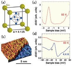
Fig. 1. (a) Schematic structure model of single-crystal SmB6. (b) Atomically-resolved STM image of the SmB6(001) surface prepared by the cycles of Ar+ sputtering and 1030 ºC annealing. (c) Spatially-averaged dI/dV spectrum over a wide range of sample bias from -3.2 V to 2.2 V at 80 K. The peak at -2 V indicates Sm termination of the prepared SmB6(001) surface. (d) Temperature dependence of the spatially-averaged dI/dV spectra on the SmB6(001) surface in the hybridization gap area at 80 K and 4.4 K. The arrow indicates the fine shoulder structure located at -15 meV possibly derived from localized bulk f-states.
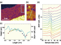
Fig. 2. (a) Atomically-resolved STM image of the SmB6(001) surface. (b) Magnified STM image of the SmB6(001) surface surrounded by blue dotted lines in (a). (c) (Left axis) STM height profile along the blue line in (b). Two types of defects, a small protrusion and a dip, are visible at ~ 0.3 (left) and at 2.2 (right) nm, respectively. (Right axis) differential conductivity dI/dV along the blue line in (b). At each position, the magnitude of the dI/dV of the peak structure located at -8 meV in (d) is plotted. (d) Series of 14 dI/dV spectra recorded along the blue line in (b). The colors indicate the recorded positions of the dI/dV spectra marked as dots with the same colors in (c), i.e, the spectra from bottom to top in (d) corresponds to the dots from left to right in (c). The dotted line indicates the energy position of a fine structure in the in-gap state.
Using STM, we have investigated structural and electronic properties of a clean SmB6(001) surface prepared by the sputtering and annealing method [3]. Our atomically-resolved observations shown in Fig. 1 (b) reveals that a non-reconstructed p(1 × 1) lattice with point defects is successfully and homogeneously formed over the entire surface using an optimal annealing temperature. In the tunneling (dI/dV) spectra on this surface, we found a peak in the density of states at – 2 eV below EF (Fig. 1(c)), which indicates the B 2p dangling bonds on a Sm-terminated surface. The hybridization gap with an in-gap state located around − 8 meV below EF develops in the tunneling spectra with decreasing temperature as shown in Fig. 1(d). In Fig. 2, we show spatial dependence of the in-gap state near EF at 4.4 K. The state is sensitive to the structural variation on the surface; it is significantly suppressed near the point defect on the ordered region, but survives on the whole surface irrespective of defects. The existence of a robust surface state, which can be an evidence of a topologically-protected surface state, is confirmed inside the Kondo hybridization gap in this system.
References
- [1] P. Coleman, Handbook of Magnetism and Advanced Magnetic Materials, 1, 95 (Wiley, 2007).
- [2] M. Ellguth, C. Tusche , F. Iga, and S. Suga, Philos. Mag. 96, 3284, (2016).
- [3] T. Miyamachi et al., Sci. Rep. 7 12837, (2017).