
Spin-Orbit Interaction in Nanoparticle-Decorated Graphene
J. Haruyama and S. Katsumoto
Introduction of spin-orbit interactions (SOIs) into two-dimensional (2D) honeycomb lattices is predicted to create 2D topological phases [1]. Graphene is a representative 2D honeycomb lattice, whereas it lacks SOIs due to the lightness of carbon atom and the complete flatness of the lattice. Though many trials to introduce SOIs into graphene with various perturbations have been reported so far, the number of sound experiments has remained small [2]. A way to introduce SOI is to distribute nanoparticle with heavy mass atoms onto graphene. Here we precisely control small-amount of nanoparticles (platinum (Pt) or bismuth telluride (Bi2Te3)) randomly distributed on graphene and observe the appearance of SOI-induced (inverse) spin Hall effect (SHE).
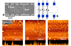
Fig. 1. (a)(b) Scanning electron micrograph and schematic top views of graphene formed into a multiple Hall bar pattern used for non-local resistance (RNL) measurements. (c -e) Atomic force microscope images of the Bi2Te3 nanoparticle decorated on graphene using a nano needle method (inset of (c)) with three different-densities (D) ; (c) – (e) for D ~ 4/(100 nm)2 (coverage ~ 3%), D ~ 10/(100 nm)2 (coverage ~ 8%), and D ~ 23/(100 nm)2 (coverage ~ 20%), respectively. Lower panels show the height along white broken lines in the upper panels.
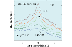
Fig. 2. Temperature variation of non-local resistance R27 as a function of in-plane external magnetic field.
Pt or Bi2Te3 nanoparticles with diameters of 3 ~ 5 nm are dispersed on monolayer graphene grown by chemical vapor deposition and formed into a multiple Hall bar (Figs. 1(a), 1(b); area for w = 2 × Lsa = 5(μm)2). High quality of the monolayer graphene has been confirmed by Raman spectra and X-ray Photoelectron Spectroscopy. The electron concentration in the graphene can be controlled with the back-gate voltage. For this experiment, we develop a specific tool, that is, a nano-needle to carry out clean and noninvasive decoration of graphene surface with nanoparticles. Dropping a small fleck of acetone, into which the nanoparticles are dispersed with ultrasound, we can precisely control the nanoparticle density (D) on the graphene surface. Examples of thus dispersed random nanoparticles are shown in Fig. 1 (c-e) for D ~ 4, 10 and 23/(100 nm2), respectively. After the decoration, samples are annealed at 400 ºC for 10 minutes under high vacuum to advance chemical bonding between the nanoparticles and the carbons.
Figures 1 (b) also shows the terminal configuration for the non-local resistance measurement. The external current is applied along 1-8, which causes the spin current along the Hall bar via the SHE. The spin current next produces voltages between 2 and 7, 3 and 6 through the inverse SHE. Figure 2 shows the temperature variation of thus measured non-local resistance R27 as a function of in-plane external magnetic field, which causes the precession of electron spins and hence diminish the non-local resistance. This can be viewed as, in a sense, a Hanle measurement. The behavior of R27 shown in Fig. 2 clearly indicates the introduction of considerably strong SOI into graphene. The estimated spin separation by the SOI is as large as 50 meV, which is the largest among so far reported. The value is supported by scanning tunneling microscopy spectra.
References
- [1] C. L. Kane and E. J. Mele, Phys. Rev. Lett. 95, 226801 (2005).
- [2] J. Balakrishnan, G. K. W. Koon, M. Jaiswal, A. C. Neto, and B. Özyilmaz, Nat. Phys. 9, 284 (2013).