
Discovery of Two-Dimensional Dirac Nodal Line Fermions in the Monolayer Cu2Si
I. Matsuda and Sugino Groups
Tremendous research interest has recently focused on topological semimetals which have vanishing densities of states at the Fermi level. In these materials, the valence and conduction bands can touch at either discrete points or extended lines. In the latter case, it forms nodal line semimetals. The band degeneracy points or lines are also protected by symmetries and are thus robust against external perturbations.
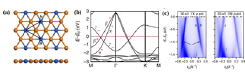
Fig. 1. (a) Atomic structure model of the monolayer Cu2Si. (b) The calculated band dispersion curves. (c) Result of the photoemission band mapping.
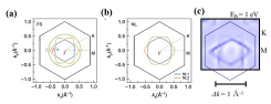
Fig. 2. (a) Fermi surface (FS), (b) nodal line (NL) of the metallic bands, α,β,γ in Fig.1. (c) Result of the photoemission band mapping for NL taken at photon energy of 30 eV and at binding energy (EB) of 1 eV.
Two-dimensional materials have also attracted broad scientific interest because of their exotic properties and possible applications in high-speed nano-devices. Thus, realization of two-dimensional topological semimetals will provide new platforms in academic and technological fields. In this work, we study monolayer Cu2Si, which is composed of a honeycomb Cu lattice and a triangular Si lattice. As shown in Fig. 1, all the Si and Cu atoms are coplanar and thus there is the mirror reflection symmetry with respect to the xy plane. This symmetric feature is significant for the existence of two-dimensional nodal lines. A commensurate monolayer Cu2Si has been synthesized on a Cu (111) surface by the Si deposition. Our comprehensive theoretical calculations show the existence of two Dirac nodal loops centered around the Γ point (Fig. 1). The gapless nodal loops are protected by mirror reflection symmetry. These characteristic band structures were directly observed by angle-resolved photoemission spectroscopy measurements (Figs. 1 and 2). The theoretical and experimental results unambiguously confirm the two concentric Dirac nodal loops in monolayer Cu2Si (Fig. 2). These results not only extend the concept of Dirac nodal lines from three- to two-dimensional materials, but also provide a new platform to realize novel devices at the nanoscale.
References
- [1] B. Feng, B. Fu, S. Kasamatsu, S. Ito, P. Cheng, C.-C. Liu, S. K. Mahatha, P. Sheverdyaeva, P. Moras, M. Arita, O. Sugino, T.-C. Chiang, K. Wu, L. Chen, Y. Yao, and I. Matsuda, Nature Comm. 8, 1007 (2017).