
Optically Detecting Edge-State of Topological Insulator under the Ambient Condition by Ultrafast Infrared Photoluminescence Spectroscopy
Suemoto and I. Matsuda Groups
Three-dimensional topological insulators (TIs) are materials characterized by insulating bulk bands and metallic surface states resulting from a nontrivial topology of the bulk wave functions. The surface states form a Dirac cone structure with electron spins locked perpendicular to their momenta within the bulk band gap. The helical spin structure, which suppresses electron backscattering induced by nonmagnetic impurities, proposes electronic and spintronic device applications of TIs. The robustness of topologically protected surface states under exposure to air furthermore offers to realize versatile TI devices operating under the ambient environment. It is therefore crucial for the device applications to investigate dynamical properties of surface carriers in TIs particularly under the ambient condition. Recently the surface carrier dynamics has been explored with ultrafast time-resolved techniques allowing for distinguishing the bulk and surface response, involving time- and angle-resolved photoemission spectroscopy (TrARPES), optical pump mid-infrared probe spectroscopy (OPMP), and optical pump THz probe spectroscopy (OPTP). TrARPES has been utilized to observe directly the transient electron population with the high momentum and energy resolution, providing knowledge about the electron-phonon scattering and the bulk-surface interband transition in TIs. TrARPES, however, needs the ultra-high vacuum condition to prevent the surface contamination of samples due to the surface sensitivity. In contrast, OPMP and OPTP have delivered insights into the low-energy electronic transition in the surface Dirac cone even under the atmospheric condition with larger penetration depth than that in TrARPES experiments, while being incapable of direct access to excited states over a wide energy range from the surface states to the bulk bands.
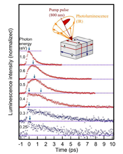
Fig. 1. Time evolution curves of the luminescence intensities from TlBiSe2 at emission photon energy ranging from 0.25 eV to 1.0 eV under 1.55 eV-photoexcitation. The curves are normalized at their own maxima and offset for clarity of display. The curves at lower photon energy than bulk band gap of 0.35 eV are shown in blue. The green arrows indicate the peak position of each curve. The inset shows schematic drawing of the infrared photoluminescence measurement under 1.55 eV (800 nm) pulse excitation.
Time-resolved photoluminescence spectroscopy (TrLS) overcomes their drawbacks with the bulk sensitivity and the wide-range detection of excited states in visible to infrared regions. TrLS combined with time-resolved photoemission spectroscopy (TrPES) has been applied to graphite, providing deep understanding on the carrier dynamics in the Dirac cone [1]. TrLS is therefore urgently expected to be a practical approach even to surface carrier transitions in TIs under the ambient consition; however, no TI research with TrLS has been reported. Here, we report an application of the infrared TrLS technique to a TI TlBiSe2 under the ambient condition (inset in Fig.1).
A TI TlBiSe2 is known to feature the Dirac point located near the middle point of the bulk band gap of 0.35 eV at the Γ point, which is a large value among TIs. We used Tl1-xBi1+xSe2 (x = 0.025) synthesized by the Bridgman method as the sample, where the Fermi-level is located near the Dirac point. The infrared time-resolved luminescence measurement was performed with the up-conversion technique under the ambient condition. The TlBiSe2 sample was excited by 70 fs pulses at a wavelength of 800 nm (1.55 eV) from Ti:sapphire regenerative amplifier operating at a repetition rate of 200 kHz. The spot size on the sample was approximately 300 μm in diameter and the fluence was estimated to be 0.34 mJ/cm2. The visible light was generated by sum-frequency mixing of the infrared luminescence light and the gating pulses at 1.55 eV in an optical nonlinear crystal LiIO3, and detected by a photomultiplier tube coupled with a double grating monochromator. The time resolution estimated by autocorrelation of the pump pulse reflected by the sample and the gating pulse was 168 fs. The energy resolution was approximately 70 meV. The up-conversion measuring system had sensitivity for the luminescence photons between 0.23 eV and 1.3 eV. The spectral sensitivity of the system was calibrated by using the sum-frequency signal between the light from a tungsten lamp with a sapphire window and the gating pulses at 1.55 eV.
Figure 1 shows time evolution curves of the luminescence intensities from the TlBiSe2 crystal at emission photon energy ranging from 0.25 eV to 1.0 eV under the 1.55 eV-photoexcitation. The decay profiles exhibit specifically different shapes with the photon energy. As photon energy decreases from 1.0 eV, the peak position time becomes longer with decrease of the photon energy. This behaviour can be explained in terms of the bulk insulating property: the carriers are accumulated at the bottom of the bulk bands due to the energy band gap, which obstructs phonon-mediated recombination between electrons and holes. The longer decay time at lower photon energy is attributed to slower relaxation of the carrier population at lower energy, reflecting the cooling dynamics of the carriers via carrier-phonon interactions. On the other hand, when the photon energy is lower than the bulk band gap of 0.35eV, distinctive decay profiles with much longer decay times (approximately 4 ps) are found at 0.25 eV and 0.3 eV. The decay profile at 0.4 eV, which corresponds to the turning point of the shape change of the decay profiles, consists of two components similar to each decay profile at 0.3 eV and 0.5 eV.
The distinctive shape change of the luminescence decay profiles and the bimodality of the time-resolved luminescence spectra elucidate that the luminescence originates from different energy bands. According to the band calculations, no bulk state resides in the energy band gap region less than 0.6 eV, except each one around the Γ point (0.35 eV) and the M point (0.3 eV)[2]. The bulk band around the M point might contribute to the luminescence at photon energy even below the bulk band gap of 0.35 eV; however, the decay profile at the photon energy of 0.3 eV that matches the energy band gap at the M point does not exhibit a rapid rise expected from the bulk insulating property [3]. The decay profiles at the photon energy below the bulk band gap of 0.35 eV are therefore attributed to the luminescence predominantly derived from the surface states. The quantitative analyses, based on the rate-equation model, also confirmed this assignment [3].
The topologically protected surface states were optically detected even under the ambient condition, and the relaxation rate of the surface carriers was determined, distinguished from the bulk contribution simply with the emission photon energy. Our results present the availability of the infrared TrLS technique as a novel approach to the dynamical properties of the surface carriers in TIs toward their application to electronic and spintronic devices operating under the ambient environment.
References
- [1] T. Suemoto et al., Phys. Rev. B 87, 224302 (2013).
- [2] K. Kuroda et al., Phys. Rev. Lett. 105,146801 (2010).
- [3] S. Maezawa et al., Sci. Rep. 5, 16443 (2015).