
Conductance Difference in the Atomic Point Contacts Formedon an Atom and Between Atoms
Hasegawa Group
Electronic conduction through atomic-size metal contacts is of fundamental interest as a transport through the ultimately squeezed conductor. Several seminal phenomena, such as quantization and step-wise variation in the conductance, have been reported using a method called break junction by measuring the conductance just before the breaking of a nanometer-width wire. In these measurements, since atomic geometry of the point contact cannot be controlled, the measured conductance fluctuates at every breaking and, therefore, the results are usually analyzed statistically using a conductance histogram.
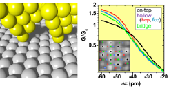
Fig. 1. (left) schematic showing the atomic geometry of the atomic point contacts formed at a on-top site (left) and a 3-fold hollow site (right) of a close-packed surface. (right) electrical conductance measured from tunneling (Δz = -20 pm) to contact (Δz = -60 pm) regimes. The measured conductance G is normalized by the quantum conductance G0 given by 2e2/h (~77.5 μS). For each conductance trace, 10 traces taken at the corresponding sites marked in the atomically-resolved STM image (inset) are averaged.
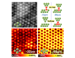
Fig. 2. Spatial mappings of the conductance at various tip displacements. (upper left) topographic STM image (3.0×3.0 nm2) taken simultaneously with 64×64 conductance traces. (lower left) conductance mapping at Δz=-32pm, where the conductance at on-top site is enhanced (lower right) conductance mapping at Δz = -60 pm, that is, the contact regime, where hollow site, particularly hcp site, has large conductance. (upper right) schematics explaining the site dependence of the conductance. The atoms on which the chemical interaction is exerted are marked red.
Here, making most of the capability of the atomically resolved imaging of scanning tunneling microscopy (STM), we directly measured the conductance of the atomic point contact in an atomically controlled manner. We first positioned the STM tip on a specific site, for instance, on-top, bridge, and hollow (fcc and hcp) sites, in the crystallographic lattice of the substrate surface, and then measured the conductance by moving the tip toward the substrate from tunneling to contact regimes. It was found that the conductance evolution depends significantly on the contact site. In the contact regime, the hollow site has the largest conductance and among the two hollow sites the hcp site is more conductive than fcc. When the tip is a little bit (20-25 pm!) far from the contact, a crossover occurs and the conductance at on-top site becomes largest.
The traces of the electrical conductance measured from tunneling to contact at on-top, bridge, fcc, and hcp sites of the Pb(111) surface are shown in the right panel of Fig. 1. For each plot, 10 traces obtained from the corresponding marked sites in the inset STM image are averaged. At the tip displacement Δz of -50~-60 pm from the tunneling (Δz = 0), the atomic contact is formed as the conductance shows saturation around the quantum conductance G0 given by 2e2/h (~77.5 μS). The contact conductance shows strong site dependence; the conductance at the hcp site is largest and more than 50 % larger than the one measured at the on-top site. Around Δz = -30~-40 pm, that is, when the tip is located above the substrate by 20~30 pm from the contact, the figure show the largest conductance at on-top site.
In order to demonstrate the site dependence, we performed real-space mappings of the conductance in the on-top enhancement region and in the contact regime. The upper-left panel of Fig. 2 is an STM image showing the atomic contrast taken simultaneously with the conductance traces. At a tip displacement Δz of -32pm, the conductance mapping (lower-left of Fig. 2) exhibits bright contrast at the on-top site, similarly to that in the topographic image. As the conductance mapping at Δz =0 does not have any contrast, the bright contrast indicates the conductance enhancement at the on-top site. On the other hand, the conductance mapping in the contact regime (lower right of Fig. 2, Δz =-60pm) has its contrast reversed from that of the topographic one, indicating a larger conductance at the hollow site than at the on-top site. These results indicate that the point contact conductance is quite sensitive to the atomic configuration.
When the distance between the tip and substrate is reduced, the attractive chemical interaction is exerted between the surface and tip apex atoms. This interaction presumably opens up the conduction channel and contributes to the development of the conductance. Schematics in the upper right panel of Fig. 2 show how the chemical interaction works in the case of contacts formed at on-top and hollow sites. When the tip approaches from the tunneling regime, the attractive interaction is exerted first at the on-top site (The force-exerted atoms are marked red in the schematics.) because the atom at on-top site is located higher than that of hollow sites, making the on-top conductance enhanced. In the contact regime, however, the attractive force becomes stronger at hollow sites because the number of involved atoms is greater than that at the on-top site. This is probably the reason why conductance becomes larger there at the contact and why the crossover occurs. Obviously further theoretical studies are needed to elucidate the observed conductance behaviors.
References
- [1] H. Kim and Y. Hasegawa, Phys. Rev. Lett. 114, 206801 (2015).