
One-dimensional Fermi Surface is Stabilized on Ge Surface Even at Low Temperature
Komori group
In solid-state physics, we learn that electrons in one-dimensional metals undergo metal-to-insulator transition induced by the Peierls instability due to electron-phonon interaction or exhibit a Luttinger liquid behavior due to electron-electron interaction with decreasing temperature. Atomic nanowires formed on semiconductor surfaces offer an opportunity to investigate such intriguing phenomena of one-dimensional metals. So far, however, their manifestations are largely disturbed by the presence of defects in the nanowires. Highly-ordered atomic nanowires at surfaces are thus essential not only for clarifying if they exhibit the Peierls instability or a Luttinger liquid behavior, but also for understanding universal nature of one-dimensional electronic systems. On the Ge(001) surface, defect- and kink-free Pt-induced atomic nanowires (Pt/Ge(001) NWs) can be formed, and are very suitable for the study of one-dimensional electrons. [1,2,3] We have investigated the ground-state electronic properties of Pt/Ge(001) NWs at the Fermi level (EF) in situ by angle-resolved photoelectron spectroscopy at 6 K, a sufficiently lower temperature than its structural phase transition at 80 K, using single-domain samples shown in Fig. 1.
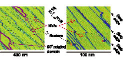
Fig. 1. STM images of Pt/Ge(001) nanowires (NW) on a vicinal Ge(001) substrate. The substrate was tilted toward the [̅110] direction by 2˚. Most of wide terraces are covered by the nanowires parallel to the step edges. The areas surrounded by purple lines in (left) represent minority domains. In both images, the bias voltage is 1.5 V and the tunneling current 0.5 nA.
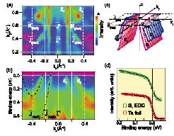
Fig. 2. (a) Constant energy ARPES intensity map at EF of Pt/Ge(001) NWs with single-domain samples formed on the vicinal Ge(001) substrate. The photoelectron intensity is represented by color scale. (b) ARPES image taken along ΓJ. Dashed curves represent the band structures of S1 and S2, which were fitted to the data. (c) Schematic illustration of the S1 and S2 bands. (d) Integrated energy distribution curve of S1 near EF over ky in the surface Brillouin zone is compared with the results of a Ta foil.
Figure 2(a) shows the Fermi-surface mapping at 6 K. Two metallic surface bands labeled S1 and S2 are clearly identified. The Fermi surface of S1 consists of straight lines in the ky direction, indicating that the S1 band disperses only in the nanowire direction. It is therefore an ideal one-dimensional metallic state which is decoupled from neighboring electronic systems. As shown in Fig. 2(b,c), it exhibits a steep dispersion and clearly crosses EF in the substrate bulk band gap. Obviously, there is no gap opening at EF. Thus, the S1 band does not directly contribute to the structural phase transition at 80 K and is stable against the Peierls instability if it exists. The electron-phonon interaction could not be strong enough to induce any structural transition with the nesting vector for S1 by the Peierls instability scheme. In order to examine a Luttinger liquid behavior, the energy distribution curve of S1 was analyzed as shown in Fig. 2(d). The observed spectral shape agrees with the normal Fermi-Dirac-type distribution function without any indication of the power-law behavior predicted for a Luttinger liquid. These novel results provide not only a valuable contribution to the phenomenology of nanowires/semiconductor systems but also a major advance for understanding the intriguing physics of the one-dimensional electrons on solid surfaces.
References
- [1] Gürlu et al., Appl. Phys. Lett. 83, 4610 (2003).
- [2] I. Mochizuki et al., Phys. Rev. B 85, 245438 (2012).
- [3] K. Yaji et al., Phys. Rev. B 87, 241413(R) (2013).