
Development of Versatile Nanoscale Potentiometry for Visualizing Distribution of Electrical Resistance
Hasegawa Group
Scanning tunneling microscopy (STM) has been utilized for imaging atomic structure of surfaces. Combined with a function of tunneling spectroscopy, the probe microscopy can also visualize spatial distribution of various properties in nanoscale; superconductivity has been detected and visualized through the observation of the superconducting gap. A spin-polarized probe tip picks up signals of local magnetization, and inelastic tunneling provides the energy of spin flipping and transition between spin states of atomic and nanosize systems. Here, we introduce another unique function of STM; mapping of electrical potential and resistance in nanometer-scale spatial resolution.
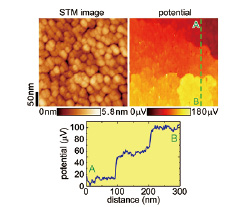
Fig. 1. STM image of a 2-nm-thick Au thin film and its potential mapping taken simultaneously under current flow (1~2 mA) from the bottom to the top of the images. A cross-sectional plot of the potential indicates that potential drops, which correspond to electrical resistance, occurs at grain boundaries and that the potential can be measured with a resolution of ~5 μV.
The method called scanning tunneling potentiometry enables us to observe spatial distribution of the the potential of a sample surface under current flow across the sample, as well as its topographic STM image. Under current flow, which is 1 ~ 2 mA in the present case, the potential or the Fermi level changes locally at the places where electrical resistance there. Figure 1 shows an example of the topographic and potential images taken simultaneously on a 2-mm-wide and 2-nm-think Au thin film. As shown in the topograph, Au grains whose size is 10 to 30 nm are randomly distributed. The potential image, however, clearly reveals steps in the potential, which provide direct evidence of significant resistance there. The sites of the drops exactly correspond to boundaries between the Au grains, as proved by a comparison of the two images. Not all domain boundaries, however, induce the potential drop, although the boundaries that induce the potential drops do not show any structural differences discernible in the STM image from those that do not induce the drops. We confirmed that the observed drops are really due to the electrical potential by taking the images under the reversed current flow across the sample; the direction of the potential drops is also reversed with the reversed current. The reversed potential image also indicates that the sites and magnitude of the potential drops do not change significantly in the both directions of the current flow.
The magnitude of the potential drops can be estimated as ~ 40 μV from the cross-sectional plot shown in Fig. 1(c). The plot also indicates that the noise level of the potential is ~ 5 μV even at room temperature. The resolution is quite high compared that of other STM-related potential measurement methods, such as Kelvin probe force microscopy, with which we detected interatomic charge transfer [1], and the method of measuring energy levels of electronic states that was used for visualizing the Friedel oscillation [2]. The reason of the high resolution is because of the zero-balance method used in the potential measurement; the potential is measured from the voltage applied on the sample to make the tunneling current zero.
One drawback is that the method can only be applied to metallic samples; in the case of semiconducting samples, the tunneling current is zero within the band gap and therefore the bias voltage that makes the tunneling current zero cannot be determined with high energy sensitivity. In this work, we have developed a new method with which one can take a potential mapping on semiconducting samples [3], which will obviously extend versatility of this technique.
We are applying the method to study potential profiles on surface conductive layers, which are the ultimate two-dimensional electron systems. Superconductivity even on one-monolayer-metal-induced reconstructed surfaces was reported. Our study will reveal roles of various structural defects on the (super-) conductance in real space. By using a spin-polarized tip, one can also detect spin current since the dispersionless current is caused by the potential difference between the two spin directions. We expect that various spin relaxation processes will be identified in real space and attributed to local structures using this method.
References
- [1] T. Eguchi, et al., Phys. Rev. Lett. 93, 266102 (2004).
- [2] M. Ono, et al., Phys. Rev. Lett. 96, 016801 (2006).
- [3] M. Hamada and Y. Hasegawa, Jpn. J. Appl. Phys. 51, 125202 (2012).