
Clustering and Merging of Vortices in Nano-Size Superconductors
Hasegawa Group
Nano-size superconductors exhibit unique properties which are different from macroscopic counterparts since the characteristic size is in the same order of the coherence length. Here we demonstrate one of them; clustered and merged vortices on Pd nano island structures observed in real space by using low-temperature scanning tunneling microscopy (STM).
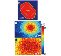
Fig. 1. (a) STM image of a Pb island structure whose thickness is 7 monolayer (2.0 nm). (b, c) mappings of the tunneling conductance at zero bias voltage taken at 0.6 T (b) and 0.7 T (c). Reddish color, indicating high tunneling conductance, shows superconductivity-broken area and corresponds to vortex (vortices).
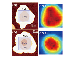
Fig. 2. STM image (left) and the zero-bias-voltage tunneling conductance image taken in the square area under 0.6 T (right) on two islands having a void structure.
When magnetic field is applied on type-II superconductors, vortices or quantized magnetic fluxes are formed. Because of the Meissner current circulating around them, these entities repel each other, and thus stabilized by forming of the triangular Abrikosov lattice. In the case of the nano-size island superconductors, the mutual interaction among the vortices is modified by the lateral confinement, and unique states or configurations which are not found in macroscopic superconductors, such as giant vortex and anti-vortex, are created.
The vortices in the Pb nano-size superconductors can be visualized by using low-temperature STM with a capability of magnetic field application. Since the superconductivity is locally broken at the core of the vortices, the position of the vortices can be directly imaged by measuring the superconducting gap at the every site by the tunneling spectroscopy. Using a 3He-cooled ultrahigh vacuum (UHV) STM setup with a superconducting magnet we have demonstrated various phenomena on the nano-size superconductors, e.g. island-size dependence of the vortex penetration field and the existence of the minimum critical size for the vortex formation, by making images showing vortex distribution of various sizes of islands as a function of the applied magnetic field.
Figure 1(a) shows an STM image of a Pb island. The island was prepared on a Si(111) substrate by depositing Pb in the UHV condition. Because of the in situ preparation, the sample is atomically flat-topped with a (111) surface and clean without any contaminations or oxide layers. From the STM image, the size, shape and thickness of the island can be measured exactly in atomic scale precision. The coherence length of 7 monolayer (ML) Pb thin film is 34 nm. Under the magnetic field, we measured tunneling spectra and mapped out the tunneling conductance at zero bias voltage, that is, at the bottom of the superconducting gap. The conductance images shown in Fig. 1(b, c) are taken in the rectangular area shown in the STM image (a) at the magnetic field of 0.6 T and 0.7 T, respectively. In these images vortices are observed as a reddish (high conductance) region around the center of the island. While the island has a circular high conductance region, which obviously corresponds to a single vortex, at 0.6 T (b), the high conductance region of 0.7 T (c) is elongated; different from the one found at 0.6 T in shape. We believe the elongated one is due to two vortices merged into a single one, that is, a giant vortex with a vorticity of 2.
These unique vortex states have been a subject of extensive studies both experimentally and theoretically. Unique capability of STM; visualizing the shape of the vortex states and configurations and directly linking them to local structures of the superconductors, will provide a significant contribution to solve the relevant issues.
References
- [1] T. Nishio et al., Phys. Rev. Lett. 101, 167001 (2008).
- [2] T. Tominaga et al., J. Supercond. Nov. Magn. (2012), DOI 10.1007/s10948-012-1522-4.