
Buckling-induced Direct π-Band Gap Opening in Epitaxial Silicene
R. Friedlein
As the Si counterpart of graphene, “silicene” may be defined as an at least partially sp2-hybridized, atom-thick honeycomb layer of Si atoms that possesses π-electronic bands [1]. Astonishing electronic properties, such as the presence of a Dirac cone, are expected to prevail even in its predicted, stable, slightly-buckled form where neighboring Si atoms are displaced out of plane [2,3]. However, different to graphene, because it can be easily buckled, silicene may exist in a variety of lattice constants, atomistic structures and with a varying sp2/sp3 ratio.
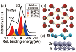
Fig. 1. (a) Surface-sensitive Si 2p spectrum recorded at normal emission. Chemical states “A” (blue), “B” (red) and “C” (yellow) have been identified by a peak fitting procedure. (b) Structure model of silicene on ZrB2(0001). (c) Calculated height profile of silicene on Zr-terminated ZrB2(0001)
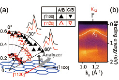 Fig. 2. (a) Intensity ratios A/B and C/B as a function of the polar emission angle (º), along the [
In a comprehensive study employing a combination of scanning tunneling microscopy (STM), angle-resolved valence band (ARUPS) and core level photoelectron spectroscopy, as well as theoretical calculations, we could 1.) demonstrate the reproducible formation of two-dimensional, epitaxial silicene on single-crystalline ZrB2(0001) thin film surfaces by segregation of Si atoms from the Si substrate, and 2.) reveal the intimate relationship between the internal structure and the electronic properties of such Si honeycomb layers [1]. Information essential to the understanding of structural details of this silicene layer has been obtained from surface-sensitive Si 2p photoelectron spectra that were recorded at the ISSP beamline 18A located at the KEK-PF synchrotron radiation facility (Tsukuba, Japan), using third-order light (130 eV).
The Si 2p spectrum obtained at normal emission, shown in Fig. 1a, indicates the presence of Si atoms in three well-defined chemical environments, labeled “A”, “B” and “C”. Within the error bars, the intensity ratio of 2:3:1 for the three components matches the single in-plane position of a Si honeycomb structure derived from STM images [1] shown in Fig. 1b. As shown in Fig. 2, diffraction of Si 2p photoelectrons originating at “A” atoms occurs on “B” along the [![]() ] direction proving the lower position of “A” atoms and atomic-scale buckling. In this structure model, the matching of the ZrB2(0001)-(2×2) unit cell with that of the Si overlayer provides a (√3× √3 ) reconstruction of silicene with a yet unpredicted buckling.
] direction proving the lower position of “A” atoms and atomic-scale buckling. In this structure model, the matching of the ZrB2(0001)-(2×2) unit cell with that of the Si overlayer provides a (√3× √3 ) reconstruction of silicene with a yet unpredicted buckling.
ARUPS spectra taken along the ![]() high-symmetry direction (Fig. 2b) show a distinct spectral feature approaches the Fermi level by up to 250 meV at the
high-symmetry direction (Fig. 2b) show a distinct spectral feature approaches the Fermi level by up to 250 meV at the ![]() point of the repeated Brillouin zone, denoted “X2” (Fig. 2b). Its upward curvature bears some resemblance to the predicted Dirac cone of π bands of freestanding, non-reconstructed silicene at its K point. It is then clear that the particular reconstruction of the silicene layer leads to a back-folding of π bands into the (now reduced) 1st Brillouin zone and the opening of a direct band gap at the
point of the repeated Brillouin zone, denoted “X2” (Fig. 2b). Its upward curvature bears some resemblance to the predicted Dirac cone of π bands of freestanding, non-reconstructed silicene at its K point. It is then clear that the particular reconstruction of the silicene layer leads to a back-folding of π bands into the (now reduced) 1st Brillouin zone and the opening of a direct band gap at the ![]() point.
point.
Bond lengths of 2.266 Å and 2.242 Å calculated for a structure that is in agreement with the experimental results (Fig. 1c) match closely to those predicted for freestanding honeycomb structures of Si [2,3]. Calculations carried out for a freestanding silicene layer with the same internal structure reveal that the opening of a gap results primarily from the particular buckling rather than from the electronic coupling to the substrate. These results imply that the atomistic structure and thus the electronic properties can be changed by the choice of appropriate substrate with selected lattice parameters, something that is (almost) impossible for the rather rigid graphene. The creation of a band gap by the control of the internal structural is likely to be fundamentally relevant for the future use of silicene in devices that perform logical operations.
Experimental help from Dr. K. Yaji and A. Harasawa (ISSP) is highly acknowledged.
References
- [1] A. Fleurence, R. Friedlein, T. Ozaki, H. Kawai, Y. Wang, and Y. Yamada-Takamura, Phys. Rev. Lett. ( to be published).
- [2] K. Takeda and K. Shiraishi, Phys. Rev. B 50, 14916 (1994).
- [3] S. Cahangirov, M. Topsakal, E. Aktürk, H. Sahin and C. Ciraci, Phys. Rev. Lett. 102, 236804 (2009).