
Field-Switchable Metal-Oxide Junctions
I. Ohkubo and M. Lippmaa
The observation of repeatable electric-field-driven switching of the resistance of metal-oxide junctions has prompted the development of resistance random access memory devices, which may allow higher-density non-volatile memories to be constructed for computing and data storage applications. The resistive switching phenomenon is known to appear at a number of oxide interfaces and various mechanisms have been proposed to explain the resistance change, including the formation of conducting filaments and the modification of the electronic or physical structure of an interface. From a solid-state physics point of view, resistive switching systems can be quite difficult to analyze, since the interface layers, while solid, are not static. High applied fields and, in filamentary conduction cases, high local current densities can result in dynamic reduction and oxidation of nanometer-scale regions, where the reaction kinetics are determined by the types of cations on either side of a junction interface and the mobility of oxygen or oxygen vacancies in the heterostructure.
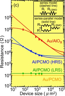
Fig.1. Device size dependence of resistance of resistive switching junctions in the low-resistance state (LRS) and high-resistance state (HRS). In LRS, contact resistance dominates, while in HRS, only a series-parallel resistance model fit (solid lines) can reproduce the observed behavior.
In this join-use project, we focus on interfaces between a semiconducting oxide, Pr0.8Ca0.2MnO3 and Aluminum metal. Under high electric fields, an electrochemical reaction can occur in solid state, resulting in the formation of an AlOx layer at the interface, which leads to the observed reversible resistance change under electric field. As a first step in characterizing the resistance switching, it is necessary to distinguish between the effects of an interface, such as trap-related Schottky barrier height changes and the formation of point-like conduction paths, which may be related to defects or inhomogeneity in the AlOx barrier that is formed at the interface during an initial field-driven oxidation process. In this project, therefore, the effect of the lateral junction dimensions on the junction resistance was studied. As illustrated in Fig. 1, the junction can be modeled as a series of two resistances for a pure interface device, but this does not adequately describe the observed device size dependence. Another possibility is to use a series-parallel model that also includes an effective inhomogeneity contribution in the form of a parasitic parallel resistance R'. As can be seen in the continuous-line fit curves in Fig. 1, this model gives a reasonable fit to the data.
It is known for the Pr0.8Ca0.2MnO3/Al system that conducting filaments do not form in the bulk of the manganites film. The junction size dependence, however, shows that a parallel conduction path does appear in the total resistance of the junctions. The most likely cause for this is the inhomogeneous field-oxidation that occurs in the junctions. In order to derive intrinsic properties of semiconductor oxide/metal interfaces, nanoscale junctions may need to be used. This work also has broader implications for the design of oxide heterostructures. It is known that growing electronically clean interfaces by typical physical vapor deposition techniques is problematic due to the large number of cations that are involved at oxide-oxide interfaces. Defect formation and interdiffusion at high film growth temperatures can set fundamental limits on the sharpness of interfaces. This work shows that functional interfaces can also be built by growing heterostructures at relatively low temperature followed by the application of an electric field to prompt the movement of anions, or even cations. The electronic properties can thus be adjusted at will at room temperature after the original heterostructure has been grown.
References
- G. Sugano, I. Ohkubo, T. Harada, T. Ohnishi, M. Lippmaa, Y. Matsumoto, H. Koinuma, and M. Oshima, Mater. Sci. Eng. B (2009), doi:10.1016/j.mseb.2009.11.022