
Transport in LaTiO3 / SrTiO3 Heterostructures
Lippmaa Group
Interface layers of transition metal oxide heterostructures offer a new playground for studying ordering phenomena and carrier dynamics in low-dimensional systems. A particularly interesting case is the combination of SrTiO3 with other insulating oxides, such as LaAlO3 or LaTiO3. It has been shown that such interfaces develop a two-dimensional high-mobility electron gas due to carriers that are accumulated in SrTiO3 close to the interface. In our work, we focus on the transport properties of LaTiO3 / SrTiO3 interfaces, which are interesting because it is possible to combine a single unit cell layer of LaTiO3 that has been predicted to show charge and spin ordering, with a 2-dimensional layer of high-mobility carriers in SrTiO3. Due to the peculiar dielectric properties of SrTiO3, it is also quite easy to modulate the density of carriers and the depth profile of carriers in the heterostructure by applying an external electric field on the heterostructure.
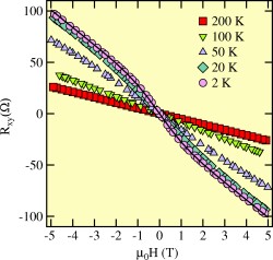
Fig.1. Temperature dependence of Hall resistance for a single monolayer of LaTiO3 embedded in SrTiO3. A fit assuming two parallel conduction paths is shown for the 2 K data.
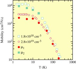
Fig.2. Temperature dependence of mobilities of an interface layer (μ1) and bulk layer (μ2) for a single LaTiO3 layer embedded in SrTiO3, compared with the mobility behavior of Nb-doped bulk SrTiO3 for two carrier densities.
We grow the heterostructures by laser molecular beam epitaxy, which allows very accurate control over layer thicknesses. Typically a single monolayer of LaTiO3 is grown on a SrTiO3 substrate surface, and finally capped with a SrTiO3 film. This produces a crystal where a single LaO atomic layer is embedded in a continuous SrTiO3 perovskite lattice. Hall effect measurements are then used to measure the density, mobility, and spatial distribution of carriers, as shown in Figure 1. At low temperatures, the Hall resistances are nonlinear, which can be understood in terms of multiple conducting layers in the heterostructures.[1] A fitting line for the 2 K data, assuming the presence of two conducting layers, is also shown in the plot. The multilayer Hall analysis allows us to extract the carrier densities and mobilities for a thin interface layer, which has a thickness of about 1 unit cell, and a thicker layer of electrons spread further into the SrTiO3 substrate, to a depth of about 10 nm. Carrier mobilities reach 104 cm2/Vs, with sheet densities in the 1013 cm-2 range.
Temperature dependence of carrier mobilities for the two layers, μ1, corresponding to a thin interface layer and μ2, which describes a thick layer of deep carriers in SrTiO3, are shown in Figure 2 and compared with the bulk mobilities of Nb-doped SrTiO3 crystals. The temperature dependence shows that the carriers at the interface follow the bulk behavior and we can thus conclude that the conducting layers are indeed in the SrTiO3 substrate. For the purpose of constructing truly 2-dimensional systems, it is necessary to eliminate the spread of carriers far into the SrTiO3 substrate. This can be done, for example by field-effect, whereby the high-mobility carriers are depleted from the heterostructure by applying a large electric field, leaving only a very thin conducting layer in the first monolayer of the substrate. Such gated structures can be used to probe interface ordering phenomena.
References
- R. Ohtsuka, M. Matvejeff, K. Nishio, R. Takahashi, and M. Lippmaa, Appl. Phys. Lett. 96, 192111 (2010).