
Nanoscale Chemical Imaging by Scanning Tunneling Microscopy Assisted by Synchrotron Radiation
Synchrotron Radiation Laboratory and Hasegawa Group
The microscopy having the spatial resolution of atomic scale with the function of element specificity is one of the ultimate microscopy for materials science. To this end, we have developed scanning tunnelling microscopy (STM) system assisted by a core-level electron excitation by synchrotron radiation light (SR)[1]. Recently, we have reported the possibility of the element-specific imaging by the SR assisted STM (SR-STM) and a quite high-spatial resolution (~ few tens nm) has been demonstrated [2]. Here, we present some more evidences of the capability of the element-specific STM observation in high-spatial resolution by the SR-STM.
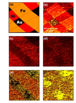
Fig.1. Images of an Fe and Ni checkerboard pattern observed by SR-STM with (b) constant current mode (topographic image), (c) photo-induced current image at hν = 706 eV and (d) 852 eV. Schematic illustration is presented in (a). Elemental specific image of Fe is presented in (e) that is obtained by dividing photo-induced current image at Fe L absorption edge top (hν = 706 eV) by that taken at edge bottom (698 eV). (f) the same as (e) but obtained with images at the Ni L absorption edge (hν = 852 /843 eV) .
The experiment was done on the beamline BL-13C at Photon Factory, KEK. As a test sample, checkerboard patterned sample consisting of Fe and Ni stripes with the thickness of about 5 and 10 nm was fabricated on a Au thick film formed on Si(100) substrate by an electron beam lithography. The width of the stripes is 1μm each. Because of the sequence of the stripe formations (Fe after Ni), Fe stripes are located at the top of the sample surface and covers partially the Ni stripes as illustrated in Fig. 1(a). The detailed setting of the SR-STM measurement is presented elsewhere [2].
In order to obtain the element specific images, we performed the STM observation during irradiating the sample surface with the SR light of different photon energies at around Fe and Ni L absorption edges. Figure 1(b) is a topographic image of the sample taken in the constant current mode by the SR-STM. We can see the checkerboard pattern clearly. Fig. 1(c) and (d) represent the photo-induced current images taken simultaneously with the topographic image at the top of Fe L3 (hν = 706 eV) and Ni L3 (hν = 852 eV) edges, respectively by using lock-in technique[2]. As shown in the figures, the photo-induced current causes significant contrast that depends on the element of the stripe structures. That is, the area of Fe is the brightest and that of Ni is the darkest in Fig.1(c) and (d). However, the photo-induced current image does not depend much on the exciting photon energies. The observed almost unchanged contrast is probably caused by the work-function difference of the materials. It has been reported that the Fe has much smaller work-function than that of Ni[3]. Since in the SR-STM measurement observed photo-induced current is dominantly due to secondary electrons which are inelastically scattered after excited by incident photons, the intensity of photo-induced current is inversely proportional to work-function and proportional to ionization cross section. The ionization cross section is nearly the same between Fe and Ni because the both two elements are neighbor in the periodic table, and the difference in photo-induced current by the work-function difference may cause the contrast.
In order to reduce the strong contrast that is not sensitive to the photon energy and to enhance the photon energy dependence, we have divided the photo-induced current image taken at the absorption edge-top by that of at the edge-bottom. Figures 1(e) and (f) are the images obtained by this procedure. In Fig.1(e), the photo-induced current image at hν = 706 eV (= edge top) has been divided by that taken at hν = 698 eV (= edge bottom). Now, as shown in Fig.1 (e), the region of Fe has larger intensity than that of Ni. Interestingly, the contrast has been inverted if we divide the images taken at the Ni absorption edge-top (hν = 852 eV) by that of the edge-bottom (hν = 843 eV) as in Fig. 1(f). This contrast inversion between the Fe and Ni absorption edges indicates that one can obtain element specific images by SR-STM by utilizing the energy tunability of synchrotron radiation.
The spatial resolution of the photo-current image can be roughly estimated by taking the intensity line profile in Fig. 1(c) along the dotted line indicated in Fig.1 (b). From the line profile (not shown here) the resolution of about 30 nm is obtained. Considering the intrinsic edge width of the patterned sample (~ 20nm) the real spatial resolution of photo-current signal can be estimated as about 10 nm [4]. The obtained value is comparable to or even better than the best spatial resolution of photoemission electron microscopy observation.
Although the mechanism of achieving such a high spatial resolution is still not clear, the local detection of the photo-induced secondary electrons through the surface barrier lowered by the proximate tip and/or via the tunneling process probably plays an important role.
References
- T. Matsushima et al., Rev. Sci. Instrum. 75, 2149 (2004).
- T. Eguchi et al., Appl. Phys. Lett. 89, 243119 (2006).
- D. E. Eastman, Phys. Rev. B 2, 1 (1970).
- T. Okuda et al., Phys. Rev. Lett. 102, 105503 (2009).