Katsumoto Group
 Research Associate ENDO, Akira
Research Subjects
- Quantum transport in charge and spin freedoms
- Study of many-body effects in quantum structures
- Physics at interfaces between the phases with different symmetries
- Quantum Hall effect
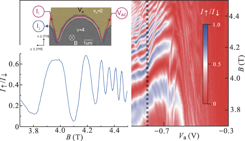
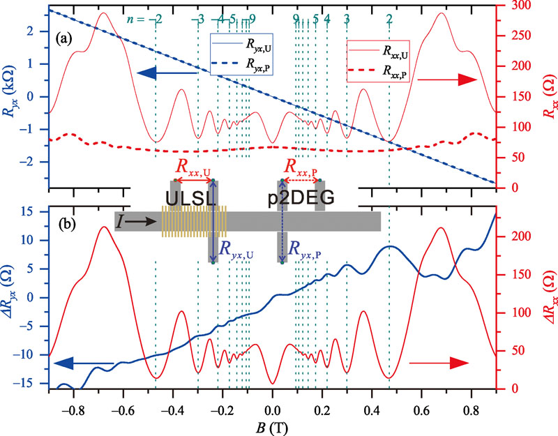
With the epitaxial growth of semiconductor and metallic films and nanofabrication techniques, we study quantum effects in low dimensional systems like quantum dots, wires and wells. Our research also spans some applications of the physics of electron and nuclear spins for so-called spintronics. To expand the concept of quantum transport to spin degree of freedom, we have tried to create spin currents in quantum structures. The nanostructures enable us to introduce new types of spin-orbit interaction by breaking the spatial inversion symmetry and creating a local orbital angular momentum. An example is the non-adiabatic unitary operation on electron spins in quantum Hall ferromagnetic edge states. Because the spin freedom and the edge states (orbital freedom) are maximally entangled in this system, the spin and the orbital operations can be utilized equivalently. Similar non-adiabatic spin rotation by the normal current can be applied to control superconductivity in a novel device.