
Spin Control in Photoemission Process from Spin-Orbital Entangled Surface States
K. Kobayashi, F. Komori, and S. Shin
Strongly spin-orbit coupled materials have been attracting much attention in solid-state physics. In particular, the potential gradient at the surface and interface largely enhances the interaction. In contrast to a conventional model with a single chiral spin texture of spin-polarized surface states, the spin-orbital texture, where spin is locked to the orbital texture of the bands, has recently been pointed out. [1] The spin-orbital entanglement is a general consequence of the strong spin-orbit coupling, and thus is important not only for surface/interface states but also bulk states, and is applicable to optical spin control in solids. However, the response of spin to light has not yet been understood fully on the basis of the quantum-mechanically entangled states with spin-orbital textures. Consequently, a clear and comprehensive concept is required on this subject. We have shown general description of the optical spin control using the spin-orbital entangled states, and demonstrated it in Bi2Se3 [2], and Bi [3] surfaces by laser-based spin- and angle-resolved photoemission spectroscopy (Laser-SARPES) [4].
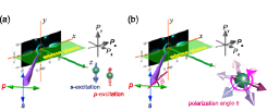
Fig. 1. Schematic illustration of photoemission processes from spin-orbital entangled surface states, where spin direction is locked in either y or –y direction, depending on the even-odd symmetry of the orbital wave functions and mirror-symmetry eigen values on the mirror-symmetry line. When the surface is irradiated by p(s)-polarized light in the mirror plane, only even(odd)-symmetry wave functions are excited, and thus, the spin direction of photoelectrons is either y or –y direction accordingly as shown in (a). When the electric field direction of light is rotated by θ from the p-polarization direction as in (b), both even and odd wave functions are coherently excited and the spin direction of the photoelectrons is determined by complex matrix elements of the photo-excitation process [2,3].
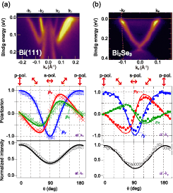
Fig. 2. ARPES of spin-orbital entangled surface states (upper), and photoelectron spin direction (middle) and normalized photoelectron intensity (lower) as a function of the angle θ of the polarization vector from the p-polarization direction shown in Fig.1(b) for the Bi(111) (a) [3] and Bi2Se3(111) (b) [2] surfaces. For Bi(111), two surface bands exist around Γ while only one band for Bi2Se3(111). Initial states of the photoelectrons are at k1 and EF for (a), and –kF for (b). The observed θ dependences are well reproduced by the formula (solid curves) using two fitting parameters of the photoemission matrix element ratio.
In the preset concept, the final state spin direction of photo-excited electrons is determined by quantum interference due to spin-locked wave functions in the optical excitation process as schematically shown in Fig. 1. On the mirror symmetry line, the spin direction of the initial state is fixed by the even-odd symmetry of the orbital wave function. In the case of SARPES measurements on the mirror symmetry line, spin direction of the photoelectron excited by linearly-polarized light depends systematically on the direction of its electric field vector, and can be expressed by the light-polarization angle (θ) from the mirror plane and a complex ratio of the dipole matrix elements from the even and odd initial states. We measured the spin direction of photoelectrons from Bi2Se3(111) and Bi(111) surfaces as a function of θ using Laser-SARPES. The results are well reproduced by the obtained formula as shown in Fig. 2 using appropriate complex values of the matrix element ratio.
References
- 1. Z.-H. Zhu et. al., Phys. Rev. Lett 110, 216401 (2013).
- 2. K. Kuroda et. al., Phys. Rev. B 94, 165162 (2016).
- 3. K. Yaji et. al., Nat. Commun. 8, 14588 (2017).
- 4. K. Yaji et. al., Rev. Sci. Instrum. 87, 053111 (2016).