
Electron-Beam-Patterned Lateral Schottky Gates on Atomically Thin MoS2
Y. Katagiri, T. Nakamura, and J. Haruyama
MoS2 is now attracting researchers’ attention among so-called “two-dimensional materials” because it has a direct bandgap of 1.5-1.8 eV in the semiconducting phase (2H, trigonal prismatic D3h). In the device application, the metallic phase (1T, octahedral Oh) part is indispensable for ohmic junctions or capacitor electrodes. The transition between the two phases does not have very high potential barrier and comparatively easily driven. Transition from 2H-phase to 1T phase caused by electron-beam (EB) irradiation has been recently observed [1].
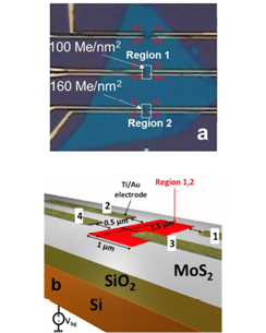
Fig. 1. (a) Optical microscope image of few-layer MoS2, mechanically exfoliated from bulk, with two EB irradiation regions and two electrode pairs patterned on individual regions. (b) Schematic view of an electrode pair on one EB-irradiated region of (a).
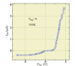
Fig. 2. Current-voltage characteristics between electrodes 3 and 4 in Fig. 1(b). The EB dose is 100 Me/nm2.
For practical device installation, a lateral Schottky barrier (SB) forming at 2H-1T interface is desirable. Hence, the EB irradiated top-down fabrication of in-plane SB field effect transistors (SB-FETs) would be promising for MoS2 based optical-electrical integrated circuits. Here we report formation of such a lateral SB junction with EB irradiation. From the current-voltage (I-V) characteristics, we believe the SB is formed at the designed position, which opens the way to 2D material integrated circuits.
Figure 1 (a) shows an optical micrograph of the sample. The MoS2 layer can be observed as a blue triangular shape. Yellow lines are Ti/Au electrodes fabricated by EB-lithography. The rectangular regions indicated by the white-broken lines are for EB irradiation, the doses of which are also indicated. The detailed electrode configuration is illustrated in Fig.1 (b). Electrodes 1 and 2 are separated from the region of irradiation while electrode 3 is attached. Hence the SB diode characteristics should appear in the transport between electrodes 3 and 4. Figure 2 shows the I-V characteristics between electrodes 3-4. Clear single SB diode characteristics appears manifesting that the SB is formed between the irradiated region and electrode 4. Note that the SB between electrode 4 and MoS2 has comparatively low resistance due to the large area and the high resistivity for the reverse bias region comes from the high quality lateral SB between the EB-irradiated 1T phase and 2H phase. The result indicates that we can make wirings and form SB-FETs at desired positions with this technique.
References
- [1] Y. C. Lin et al., Nature Nanotech. 9, 391 (2014).
- [2] Y. Katagiri et al., Nano Lett. (2016) (doi: 10.1021/acs nanolett.6b01186).