
Distant-Dependent Tunneling Process Observed in Iron Nitride
Komori Group
Scanning tunneling microscopy (STM) is one of the most powerful tools to investigate surface topographic and electronic structures with an atomic resolution. Surface nanostructures are often discussed based on the topographic image. However, its image contrast is mainly based on the electron tunneling processes between the STM tip and the surface local electronic states [1]. Systematic changes of the image contrast as a function of the sample-bias voltage Vs have been widely interpreted in terms of energy-dependent electronic structures. The STM tip-surface distance, d, is an alternative parameter of the image change on the surface consisting of several orbitals with different decay lengths of the wave functions into the vacuum. In such systems, the image can be changed by the shift of the dominant surface orbital contributing to the tunneling process. We have demonstrated the d-dependent STM imaging and spectroscopy on the surface of a monatomic layer of iron nitride (Fe2N) on Cu(001) (see Fig. 1) to characterize the orbital-sensitive tunneling as the origin of the topographic image changes [2].
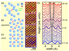
Fig. 1. (a) Schematic model of an Fe4N crystal. The layer consisting of Fe2N stoichiometry, indicated by green lines, appears at the surface of the Fe4N thin films on Cu(001). (b,c) Schematic surface models of the p4gm(2x2) reconstruction (b) corresponding to the monatomic Fe2N layer on Cu(001), and c(2x2) reconstruction (c) corresponding to the ideal bulk Fe2N plane. (d-g) Topographic images taken at Vs = 0:25 V with varying It from 0.1, 3.0, 10 to 45 nA. (h) Line profiles at Vs = 0:25 V, measured along lines indicated in (d-g). From the top to the bottom, I varies as follows: 45, 40, 35, 30, 28, 25, 22, 20, 18, 15, 12, 11, 10, 9.0, 8.0, 7.0, 5.0, 3.0, 2.0, 1.0, 0.9, 0.8, 0.7, 0.6, 0.5, 0.4,.0.3, 0.2, and 0.1 nA, respectively. Empty circles indicate peak positions extracted from one Fe dimer.
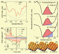
Fig. 2. (a) dI/dV spectra of Fe2N on Cu (001) and the clean Cu(001) surface. The STM tip was stabilized at It = 30 nA and Vs = 1 V. (b) Calculated spin-resolved LDOS of single-layer Fe2N on Cu(001). Fe and N states are separately shown. (c) Distant-dependent dI/dV spectra measured at d = 0.42, 0.34, and 0.29 nm from the bottom to the top. Dashed curves indicate a tunneling background obtained by a Tersoff-Hamann approximation. [1] (d-f) Topographic images taken at Vs = 0.25 V with d = 0.29 nm (d), 0.34 nm (e), and 0.42 nm (f).
Figure 1(d-g) shows a systematic change of the topographic images of the Fe2N layer from a dimerized atomic image reflecting the atomic surface structure to a square lattice of atomic size dots with increasing d. The line profiles shown in Fig. 1(h) are systematically changing with the tunneling current. By measuring the images with various VB values, the threshold distance of the image change was found to be independent of VB . The tunneling spectrum on the Fe2N surface has several peaks that well correspond to the peaks of the calculated total local density of states (LDOS) as in Fig. 2(a,b). The observed systematic d dependence of the tunneling spectra shown in Fig. 2(c) implied the shift in the dominant electronic states contributing to the tunneling process. The LDOS calculations above the surface by first principles indicate the change of the dominant orbitals detected by the STM tip from the Fe 3d states to the s/p states with increasing the tip-surface distance.
References
- [1] J. Tersoff and D. R. Hamann, Phys. Rev. B 31, 805 (1985).
- [2] Y. Takahashi et. al., Phys. Rev. Lett. 116, 056802 (2016).