
Band-Gapped Graphene Nanoribbons Made by Molecular Beam Epitaxy
S. Tanaka and F. Komori
Graphene nanoribbons (GNRs) are attracting much attention in solid state physics and nanoelectronic applications, where the band-gap opening or modification of the electronic structure at K-points is a central interest. The electronic structure at K-points in GNRs has been theoretically shown to depend on the type of edge geometry: armchair or zigzag [1]. Semiconducting characteristics are expected in the case of armchair edges owing to the band-gap opening at K-points. As the width of GNRs is reduced, the gap is increased by both electron confinement and edge effects. However, realization of GNRs with atomically well-defined edges and providing experimental evidences of the gap opening at K-points remain challenging. Here we demonstrate a new approach for producing a dense array of aligned GNRs on unique SiC surfaces [2] as templates via molecular beam epitaxy (MBE), and show band-gap openings at K-points visualized by angle-resolved photoemission spectroscopy (ARPES) [3].
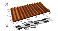
Fig. 1. (a) An AFM 3-dimensional view of the vicinal SiC(0001) surface after hydrogen etching, showing a periodic array of terrace and facet structure. (b) A schematic drawing of the SiC surface in (a). This was derived from high-resolution transmission electron microscopy images. Each pair of array consists of the (0001) terrace and (1-10n) facet, and is ordered with the periodic distance of ~ 20 nm. Here, n = 35 ~37. The width of each (0001) terrace is ~ 10 nm.
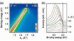
Fig. 2. Intensity map (a) and energy distribution curves (EDCs) (b) of the ARPES spectra around the K-point for the GNRs on the vicinal SiC(0001) substrate. The spectra are taken along the Γ-K-M line. The EDCs show the folding of the valence band at the K-point below EF. The red dots in (a) indicate the positions of the EDC peaks and represent band dispersion around the K-point. The intensity map indicates a linear dispersion, which is consistent with the valence band of single-layer graphene.
In the present study, we used an off-axis SiC substrate (Si-face, 4º off toward [1-100]), and first prepared a self-ordered periodic structure consisting of pairs of a (0001) basal plane terrace and a (1-10n) nanofacet (n = 35~37) with a characteristic periodicity of ~ 20 nm by H2 gas etching [2]. A typical atomic-force-microscopy (AFM) image of the substrate and a model are shown in Fig. 1. After cleaning the surface of the substrate under Si flux at 1050ºC, a carbon mono-atomic layer with (6√3×6√3)R30º registry was grown exclusively on the SiC terrace by MBE. Finally, the samples were exposed to H2 gas at 600ºC for 1 h to transform the carbon layer into quasi-free-standing graphene by hydrogen intercalation. The GNRs thus made have armchair edges parallel to the step edge of the substrate. Quality of the graphene was evaluated by AFM, scanning tunneling microscopy, reflection high-energy electron diffraction, low-energy electron diffraction, and Raman spectroscopy.
Figure 2(a) shows the ARPES result along the Γ-K-M lines of the graphene surface Brillouin zone. The measured Γ-K-M direction in k-space corresponds to the [1-100] direction in real space, which is perpendicular to the edges of the GNRs. A conduction band is invisible, and the valence band is folded at the K-point area, as shown in Fig. 2(b). No states are detected at the K-point between the Fermi energy (EF) and top of the valence band, which is 0.14 eV below EF. The band-gap value can be more than 0.28 eV if we assume a slight p-type doping in the sample as in the case of the hydrogen-intercalated graphene on SiC(0001). This value is consistent with the theoretical estimation for the GNR with the width of 10 nm.
References
- [1] K. Nakada et. al., Phys. Rev. B 54, 17954 (1996).
- [2] H. Nakagawa et. al., Phys. Rev. Lett. 91, 226107 (2003).
- [3] T. Kajiwara et. al., B 87, 121407(R) (2013).