
Bias-Dependent Atomic STM Images and Electronic Structure at Au-Adsorbed Ge(111) Surface
Komori Group
The Au-adsorbed Ge(111) surface has two surface metallic bands with hexagonal Fermi surfaces [1]. One band is electron-like and the other is hole-like. The former band is anisotropically split and spin-polarized owing to strong spin-orbit interaction at the surface. These features have been studied by angle-resolved photoemission spectroscopy (ARPES). Figure 1(a) shows the ARPES intensity map along Γ0 − M − Γ1 line for the surface with 0.9 ML of Au on average. The observed electronic states including the surface bands (S1, S2 and S5) are qualitatively consistent with the bands calculated for an optimized conjugate honeycomb-chained-trimer (CHCT) structure model shown in Fig. 1(b) [2]. However, there have been two discrepancies between the experiments and theories; the STM image at low bias voltage (Vsb) and the bottom energy of the S1 band. In the present study, we clarify how these are solved by considering the surface electronic structure and the doping by triangular nanoclusters observed on the surface.
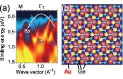
Fig. 1. (a) ARPES intensity map showing the band structure of the Au-adsorbed the Ge(111) surface. Three surface bands S1, S2 and S5 are seen, and white dashed lines are guides to the eye for the S1 and S2 bands. (b) Schematic top-view CHTC model for the Au-adsorbed Ge(111) surface. The white hexagonal lattice indicates the subsurface bilayer Ge lattice, the small blue balls the lower Ge atoms of the bilayer, small green the upper Ge atoms of the bilayer, yellow the surface Ge atoms, and red the surface Au atoms. Three adjacent Au atoms make an Au trimer, which is imaged as a single protrusion in Fig. 2(a). Centers of three adjacent Ge atoms are imaged as protrusions in Fig. 2(b), and make a honeycomb pattern, which is indicated as the magenta hexagon
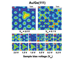
Fig. 2. STM images of the Au-adsorbed Ge(001) surface showing sample-bias-voltage (Vsb) dependence. Triangle lattice pattern in (a) is attributed to the arrangement of the surface Au trimers. (See Fig. 1(b)). In (b), atomic protrusions arrange in a honeycomb pattern. The same area is imaged in (a) and (b). A triangular nanocluster is seen as a protrusion in (a) while it is imaged as a dented area in (b). The precise bias dependence of the lattice pattern and the triangular nanocluster is shown in (c-h) and (i-n). Both the triangle and honeycomb patterns coexist for Vsb = 0.5 V as in (f). The triangular nanocluster becomes thin with decreasing Vsb.
Figure 2 shows bias-dependent atomic STM images. The images were observed at 80 K for the surface with 1.2 ML of Au atoms on average. The STM image for Vsb = 2.0 V (Fig. 1(a)) shows a triangle lattice pattern with a triangular nanocluster. For Vsb = 0.1 V (Fig. 1(b)), a honeycomb pattern appeared on the same surface area, and the position of the triangular nanocluster was imaged as a dented area. The triangle lattice is consistent with the arrangement of the Au trimers on the surface in the CHCT model shown in Fig. 1(b) whereas the honeycomb pattern could not be attributed to any arrangement of the surface Au and Ge atoms in the model. Bias-dependent STM images shown in Figs. 2(c-h), and 2(i-n) indicate gradual change of the lattice pattern and the triangular nanocluster, respectively.
It was theoretically shown that the surface Au trimers of the CHCT model make the electron-like (S1) band. The hole-like (S2) band, on the other hand, originates from the surface and subsurface Ge atoms. The energy maximum of the S2 band is 0.1 eV above Fermi energy. Consequently, the local density of states around the surface Ge atoms can be high at the top energy of the S2 band. This causes a honeycomb lattice pattern of the protrusions due to the surface Ge atoms in the STM images as observed for Vsb < 0.3 V. The bottom of the S1 band decreases with increasing the surface density of the triangular nanocluster. It plays a role of the dopant selective to the S1 band although its atomic structure is unknown [3].
References
- [1] K. Nakatsuji et. al., Phys. Rev. B 80, 081406 (2009).
- [2] K. Nakatsuji et. al., Phys. Rev. B 84, 035436 (2011).
- [3] K. Nakatsuji et. al., J. Phys. Condens. Matter 25, 045007 (2013).