
One-dimensional Fermi Surface for an Anisotropic Two-dimensional Metallic State at Au-adsorbed Ge(001) Surface
Komori Group
Electronic structure of the Au-adsorbed Ge(001) surface with a one-dimensional (1D) atomic structure has been studied as one of the low dimensional metallic states. A 1D metallic state was claimed on the basis of the results of scanning tunneling spectroscopy and Fermi surface mapping [1] while the metallic state shows anisotropic two-dimensional dispersion in the study of angle-resolved photoemission spectroscopy (ARPES) [2]. The exact position of the band bottom in the surface Brillouin zone (SBZ) and the direction of the strong dispersion have not been fixed because the surfaces with two domains on a flat Ge(001) substrate were used in all the previous experimental studies. We have studied the electronic states by ARPES using single-domain samples on a substrate tiled to the [110] direction to understand this interesting low-dimensional system.
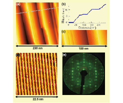
Fig. 1. (a) STM image of a Au-adsorbed vicinal Ge(001) surface, which consists of (001) areas with Au-induced chains and step-bunched areas. Gold was deposited on the clean substrate of 4 degree off to the [110] direction at 740 K, (b) Cross section along the dotted white line in (a). A step-and-terrace structure is evident. (c) Magnified STM image of a part of the surface shown in (a). Gold-induced chains parallel to the step edges are seen on the (001) surface. No periodic structure was observed on the step-bunched areas. (d) Atomic image of the chain structure on the (001) terrace. The sample bias voltage was −1 V. Eight-fold periodicity in the chain direction is clearly shown as the presence of the dots in the groove between the chains. (e) Typical LEED pattern of the single-domain surface at 60 eV.
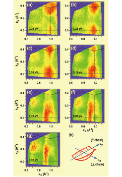
Fig. 2. (a-g) Constant-energy ARPES intensity maps of the metallic band around (kx, ky) = (0.98 Å-1, 0 Å-1) for the binding energy = 0.28 (a), 0.22 (b), 0.18 (c), 0.14 (d), 0.10 (e), 0.06 (f) and 0.02 eV (g). The chain direction is parallel to ky. The ARPES intensity is plotted after normalization of each spectrum by its total intensity. The width of the energy window is 20 meV. Intensity is the highest in the red area, and the lowest in the green area. Dispersion in the chain direction is smaller than that in the direction perpendicular to the chain. (h) Schematic model of the metallic band.
Figure 1 shows the results of scanning tunneling microscopy (STM) and low energy electron diffraction. They indicate the formation of the single-domain surface with the well-known atomic chain structure that is commonly observed on the flat substrates [3]. The surface consists of the chains parallel to the step edges. The separation of the adjacent chains is 1.6 nm, and an 8-fold periodicity can be seen in the chain direction. The symmetry of the surface structure has been considered to be c(8x2) while some of the observed LEED spots do not belong to this symmetry. [2]
Constant-energy ARPES intensity maps of the metallic band for a single-domain surface are shown in Figs. 2(a-g). The band bottom of the metallic state is found at the zone boundary (![]() point) of the c(8x2) SBZ as in Figs. 2(a-d). The band shows dispersion in the both parallel and perpendicular directions to the chain. (Fig. 2(d-f)) Contrary to our intuitive expectation, direction of the strong band dispersion is perpendicular to the chain. At the energy close to EF, the band is almost parallel to the chain as in Fig. 2(g) just like a 1D electronic state in the direction perpendicular to the chain. A schematic model of the metallic band is shown in Fig. 2(h). This state has a very unique band shape.
point) of the c(8x2) SBZ as in Figs. 2(a-d). The band shows dispersion in the both parallel and perpendicular directions to the chain. (Fig. 2(d-f)) Contrary to our intuitive expectation, direction of the strong band dispersion is perpendicular to the chain. At the energy close to EF, the band is almost parallel to the chain as in Fig. 2(g) just like a 1D electronic state in the direction perpendicular to the chain. A schematic model of the metallic band is shown in Fig. 2(h). This state has a very unique band shape.
References
- [1] S. Meyer et.al. Phys. Rev. B 83,121411(R) (2011).
- [2] K. Nakatsuji et.al., Phys. Rev. B 80, 081406 (2009).
- [3] R. Niikura et.al., Phys. Rev. B 83, 035311 (2011).