
Halide Perovskite Thin Films for Photovoltaics
K. Kawashima, R. Takahashi, and M. Lippmaa
Structurally similar to classical perovskite oxides, organic halide perovskites have a general formula ABX3, where the anion X can be I, Br, or Cl, the B-site is occupied by Pb, and the A-site usually holds the methylammonium ion, CH3NH3. Halide perovskites are studied as energy harvesting materials in photovoltaics, achieving solar cell energy conversion efficiencies of around 20%. A major technical problem with perovskite solar cells is the low structural stability of the halide perovskite material. The carrier mobility and recombination rates therefore quickly degrade after film growth. The purpose of this collaboration project was to develop a technique for quickly fabricating organic halide perovskite thin films with controlled composition and layer thickness to optimize the material characteristics. A pulsed molecular beam epitaxy system with continuous wave infrared heating (cwIR-MBE) was designed to tackle this problem. The thin film growth system is shown in Fig. 1a, showing two precursor cells containing the PbI2 and CH3NH3I precursors on a rotatable target stage. The stage can be used to position either one of the sources to face directly the substrate. A cw infrared laser is used to briefly heat the source cell in front of the substrate, yielding a millisecond-scale pulsed MBE process. The amount of material evaporated can be controlled by tuning the laser power, pulse length, and the evaporation pulse count. The main benefit of the technique is that the evaporation is thermal, not ablative, which means that the organic precursor material is not decomposed in the evaporation process. Periodically evaporating either of the two sources is used to obtain the desired PbI2 and CH3NH3I layer sequence. A homogeneous perovskite phase can be obtained if the individual layer thicknesses are limited to just a few unit cells and the average stoichiometry is close to the desired value.
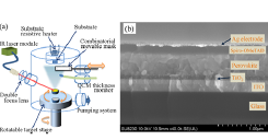
Fig. 1. (a) Schematic view of the pulse MBE deposition system. (b) A cross-sectional image of a completed organic halide perovskite solar cell.
This thin film growth system was used to fabricate arrays of perovskite solar cells, integrating several devices with slightly different precursor ratios on a single substrate to minimize statistical errors in the device characterization. A cross-sectional view of a completed solar cell device is shown in Fig. 1b. X-ray diffraction analysis was used to determine the optimal evaporated precursor ratio to obtain the perovskite phase. The total film thickness analysis was used to confirm that homogeneous phase formation occurs in multilayer films where the PbI2 and CH3NH3I layer thicknesses are 1.4 nm and 1.7 nm, respectively. Characterizing a series of solar cells showed that even in the screening experiment, a device efficiency of 10 % could be achieved.
The success of the halide perovskite synthesis by IR-MBE shows that sequential evaporation of organic precursor sources is an effective way of depositing nanometer-scale layers of volatile organics in a physical vapor vacuum process. The geometry of the evaporation process is arranged so that each target is directly facing the substrate during evaporation, which minimizes spatial layer thickness gradients on the sample surface. Additionally, only a single laser is required to evaporate several different precursor materials, while the necessary heating power and pulse length can be adjusted individually for each precursor material. The work thus shows that organic multilayer and homogeneous phase materials can be grown in a technically simple sequential MBE chamber.
References
- [1] K. Kawashima, Y. Okamoto, O. Annayev, N. Toyokura, R. Takahashi, M. Lippmaa, K. Itaka, Y. Suzuki, N. Matsuki, and H. Koinuma, Sci. Tech. Adv. Mat. 18, 307 (2017).