
Nanocomposite Electrodes for Photoelectrochemical Water Splitting
Lippmaa Group
Photoelectrochemical water splitting can be used to harvest solar energy and produce hydrogen gas, which can be stored for later use in a fuel cell to generate electricity or used as a raw material for chemical synthesis. A major obstacle to wide-spread solar hydrogen production is the low efficiency of the energy conversion process due to large recombination losses in typical water-stable oxide semiconductors, such as titanates. In a typical oxide semiconductor, illustrated in Fig. 1a, a band bending region exists at the oxide-water interface, where electron-hole pairs are formed by light excitation and separated by the internal electric field. For an n-type semiconductor, photogenerated holes would be transported through a surface depletion layer to the surface, where the oxygen evolution reaction can take place. Hydrogen would be produced on a suitable counter electrode. However, only photocarriers formed within a few tens of nm of the surface can escape from the semiconductor and participate in water splitting, whereas photocarriers formed deeper in the semiconductor are rapidly lost to trapping and recombination. Considering the visible light absorption length, which is closer to micrometer scale in doped titanates, the fraction of incident light that can actually be converted to active photocarriers at the surface is on the order of a percent.
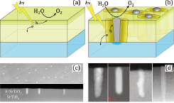
Fig. 1. (a) Operating principle of a photocatalytic energy conversion system where photogenerated charges are extracted only from a thin surface layer. (b) A nanopillar composite electrode where tubular Schottky junctions surrounding metal pillars extend the charge extraction region to the full depth of a thin film electrode. (c) Plan and cross-section STEM views of Ir metal nanopillars in a Ir:SrTiO3 matrix, (d) Examples of (left-to-right) Ir, Pt, Pd, and Rh nanopillars grown in a SrTiO3 matrix. The diameter of all pillars is 5 to 10 nm.
Various strategies exist for improving the charge extraction efficiency from oxide photoelectrodes. Besides a pure materials approach directed at finding more efficient semiconductors and doping schemes, it is also possible to design suitable nanoscale structures that improve charge collection by virtue of geometric effects. In our work, we have developed a method of growing noble-metal-doped titanate semiconductors where some of the noble metal segregates in the form of nanoscale pillars as illustrated in Fig. 1b. When the nanopillar consists of a high work function metal and the surrounding semiconductor is an n-type material, tubular Schottky junctions form around each pillar. The internal field of the Schottky junction ensures efficient charge separation and extraction throughout the thickness of the thin film photoelectrode, while the metal nanopillars provides a low-resistance charge extraction path to the film surface.
The formation of noble metal nanopillars is achieved by considering the kinetic and thermodynamic crystal growth parameters in a pulsed laser deposition process. For several noble metals, it is possible to find a balance between the oxidation rate of the metal and the growth rate of the crystal, where the average background oxygen pressure is low enough for metal segregation to occur at the initial growth stage of a film and the growth rate is balanced with the surface migration rate so that further segregated metal can form vertical pillar structures.
From the point of view of water splitting, the best starting material for the nanopillar composite photoelectrode growth is Ir:SrTiO3. Homogeneously doped Ir:SrTiO3 is an n-type semiconductor, while bulk iridium metal is a high workfunction material, ensuring that Schottky junctions form at Ir – Ir:SrTiO3 interfaces. Additionally, Ir and IrO2 are electrocatalysts that are known to promote the oxygen evolution reaction in water. The formation of segregated Ir metal inclusions in a Ir:SrTiO3 film can be seen in scanning transmission electron microscope (STEM) plan and cross-section views in Fig. 1c. The cross-section image shows that the pillars do indeed nucleate at the SrTiO3 substrate interface, and that approximately 10 nm wide pillars extend through the thickness of the film to the photoelectrode film surface. The spontaneous segregation behavior seen for Ir can be reproduced for a variety of noble metals. Although the particular growth parameters vary from metal to metal, nanopillar formation has been observed for Ir, Pt, Pd, and Rh (Fig. 1(d)).
References
- [1] S. Kawasaki, R. Takahashi, T. Yamamoto, M. Kobayashi, H. Kumigashira, J. Yoshinobu, F. Komori, A. Kudo, and M. Lippmaa, Nature Commun. 7, 11818 (2016).