
Periodic Modulation of Local Density of States at a Ge Surface with One-dimensional Atomic Structure
Komori Group
One-dimensional (1D) atomic structures often appear on metal1 adsorbed semiconductor surfaces, where we can expect interesting 1D electronic propertyies. We have studied local atomic and electronic structures of the Au-adsorbed Ge(001) surface with a one-dimensional chain structure in the <110> direction using scanning tunneling microscopy (STM) at 80 K. The period of the chain in the perpendicular direction is 1.6 nm, which is the quadruple length of the substrate Ge(001)-1 × 1 lattice constant. Figure 1(a) shows an STM image of the top of the chains at this surface. The groove between the adjacent chains is deeper than 0.3 nm, and it is difficult to observe atomic images in the grooves by STM. Previous angle-resolved photoemission spectroscopy (ARPES) studies [1,2] demonstrated a metallic surface state with the bottom binding energy about 0.15 eV below Fermi energy EF while the direction of the strong dispersion is under debate because of the use of double domain samples in these experiments.
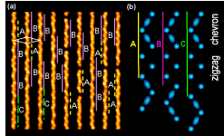
Fig.1.(a) High-resolution topographic STM image showing protrusions on top of the chains on the surface. The image was taken at 80 K with the sample bias voltage Vb of − 1.0 V. Typical arrangements of the protrusions in the chain direction are indicated by dotted, solid and dashed lines A–C. They consist of a chevron unit and zigzag structures with different lengths. Among these arrangements, the B type is most frequently seen on the surface. The length of line B is 3.2 nm, eight times of the Ge(001) 1 × 1 lattice constant. A very local c(8×2) arrangement of the zigzag structure is indicated as the white diamond. (b) Schematic models of the three common arrangements of the protrusions consisting of a chevron unit and zigzag structures. Models A–C correspond to arrangements A–C in (a). The total length increases with increasing length of the zigzag structure.
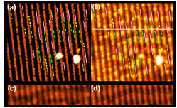
Fig.2. (a,b) STM images of the surface showing arrangements A–C of the chain protrusions for (a) Vb = − 1.0 V and (b) Vb = − 0.2 V. Dotted, short solid and dashed lines indicate arrangements A, B and C of the chevron unit and the zigzag structure given in Fig. 1(b), respectively. (c,d) Magnified STM images of the same area as that between the two horizontal white lines in (b) for (c) Vb = + 0.1 V and (d) Vb = + 0.3 V.
The top of the one-dimensional chain shown in Fig. 1(a) consists of a chevron unit of the protrusions and zigzag structures. There are characteristic combinations of the chevron unit and the zigzag structure with different lengths, which are marked as the lines A-C in the figure. Schematic models of these combinations are given in Fig. 1(b). Model B occurs most frequently on the surface, and gives an eight-fold superstructure in the chain direction.
A modulation of the local density of states in the chain direction was observed by STM for a sample bias (Vb) region between − 0.2 and + 0.6 V as shown in Fig. 2(b) for Vb = − 0.2 V. Only the surface metallic band was detected by ARPES between EF and EF − 0.2 eV. Thus, the modulation shown in Fig. 2(b) is attributed to the metallic band. By comparing the Figs. 2(a) and 2(b), the local density of state is lower at the chevron unit than the zigzag structure for the electron energy between EF and 0.2 eV below EF. The local density of states is also lower at the chevron unit in the empty state as in Fig. 2(c,d). The surface metallic state has an eight-fold charge modulation in the chain direction.
References
- J. Schäfer, et. al., Phys. Rev. Lett. 101, 236802 (2008).
- K. Nakatsuji, et. al., Phys. Rev. B 80, 081406 (2009).