ナノスケール人工物質・表面・界面の物性
構成原子の種類と並び方を高度に制御した人工低次元系、ナノメートルスケールの周期構造をもつ系、原子レベルで制御された様々な固体表面や界面では、その新奇な構造のために、興味深い電気的磁気的性質や化学反応性が現れてきます。そこで、最新の超高真空技術、微細加工技術、顕微鏡技術などを駆使して、金属、半導体、酸化物からなる新奇な物質を創成し、それが生成される機構やそこに現れる物性の起源をミクロに解明することを目標に 研究を行っています。また、そのような研究を推進するための新しい実験手法や観測された物性を利用し役立てるための素子作製方法などの技術開発も行っています。
Nanoscale materials, surfaces, and interfaces
Novel electronic, magnetic, and chemical properties appear in atomically well-defined artificial low-dimensional, nanoscale-periodic, and surface/interface systems because of their unique structures. We are studying these systems of metals, semiconductors, and oxides to elucidate their formation mechanisms and fundamental material properties microscopically using modern ultra high vacuum, micro fabrication, and microscopy technologies, and so forth. We are also developing new experimental methods for these studies and investigating ways to utilize the newly found properties of these systems for fabricating new devices.
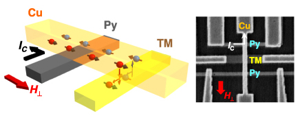
スピン吸収法を用いた遷移金属のスピンホール効果測定。
Measurement of spin Hall effect in transition metal using the spin absorption technique.
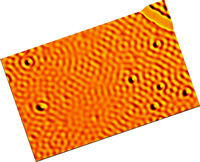
走査型トンネル顕微鏡を用いて銅表面で観察される電子定在波。
Electron standing waves on a Cu surface observed by scanning tunneling microscopy (STM).
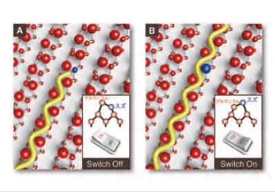
半導体表面上の原子対の傾きをパルス電流を用いて局所的に変化させ,表面を流れる電流をスイッチする。
One-dimensional electronic conduction is switched by locally changing the tilting direction of a pair of surface atoms using a pulsed current.
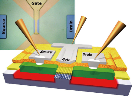
酸化物極薄膜電界効果トランジスタ
Oxide thin film FET
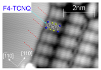
Cu(100)表面のステップ下端に選択的に吸着する強力なアクセプター分子F4-TCNQのSTM像。
STM image of strong acceptor F4-TCNQ molecules preferentially adsorbed at a lower step edge on Cu(100).