
ナノスケール人工物質・
表面・界面の物性
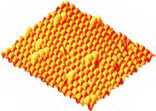
構成原子の種類と並び方を高度に制御した人工低次元 系、ナノメートルスケールの周期構造をもつ系、原子レベ ルで制御された様々な固体表面や界面では、その新奇な 構造のために、興味深い電気的磁気的性質や化学反応性 が現れてきます。そこで、最新の超高真空技術、微細加工 技術、顕微鏡技術などを用いて、金属、半導体、酸化物から なる新奇な物質を創成し、それが生成される機構やそこ に現れる物性の起源をミクロに解明することを目標に研 究を行っています。また、そのような研究を推進するため の新しい実験手法や観測された物性を利用し役立てるた めの素子作成方法などの技術開発も行っています。 。
Nanoscale materials,
surfaces, and interfaces
Novel electronic, magnetic, and chemical properties appear in atomically well-defined artificial low-dimensional, nanoscale-periodic, and surface/interface systems because of their unique structures. We are studying these systems of metals, semiconductors, and oxides to microscopically elucidate their formation mechanisms and fundamental material properties using modern ultra high vacuum, micro fabrication, and microscopy technologies, and so forth. We are also developing new experimental methods for these studies and investigating ways to utilize the newly found properties of these systems such as for fabricating new devices.
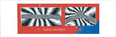 スピン渦構造の電子線ホログラム
パーマロイ強磁性ナノ細線中に生成したスピン渦構造の電子線ホログラム.図 中の黒と白の線の流れは磁力線の分布に相当する.
Electron holograms of spin vortices
Electron holograms of spin vortices nucleated in ferromagnetic permalloy nano wires 500 nm wide and 30 nm thick. Black and white lines in the figures correspond to the magnetic flux lines.
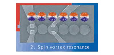 静磁的に結合したスピン渦鎖の共鳴測定用素子
磁気渦の共鳴振動が静磁気的に結合したスピン渦鎖を伝搬する様子を電気的に 計測する素子の走査電子顕微鏡像.内装図は,スピン渦の数値計算結果を示す.
A device for observing resonances in a magnetically coupled spin vortex chain
Scanning electron micrograph of a device used to observe spin vortex resonance propagating along a magnetically coupled spin vortex chain. The inserts indicate numerically calculated spin vortex structures.
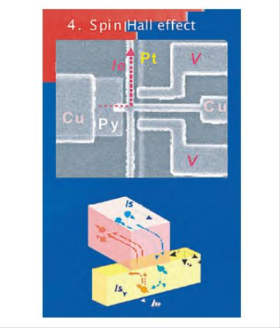 スピンホール効果と素子
非局所スピン注入によって誘起された純スピン流は,白金ナノ細線中でスピン ホール効果を通じて電流に変換され電圧信号として検出される.
A device for measuring the spin Hall effect
Pure spin current, induced by non local spin injection, is converted into charge current via the spin Hall effect in a platinum nano wire, which is detected as a voltage drop along the wire.
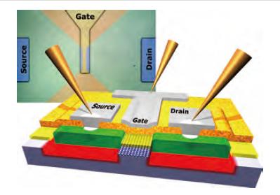 酸化物極薄膜電界効果トランジスタ
電界効果を利用して酸化物界面・薄膜のキャリア濃度を変調し,物性を調べている.
Oxide thin film FET
We are studying phase transitions in oxide heterostructures by electric field-effect doping.
 自己集積した窒化マンガンナノ粒子配列
原子サイズの界面格子歪み緩和現象を利用して,銅表面上に窒化マンガンナノ 粒子を規則的に配列させた.
Self-assembled array of MnN nanodots
Using the interface strain relief of two lattice-mismatched materials, a MnN nanodot array is fabricated on a Cu surface.
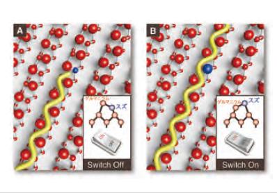 半導体表面上の原子スイッチ
半導体表面上の原子対の傾きをパルス電流を用いて局所的に変化させ,表面を 流れる電流をスイッチする.
Atomic seesaw switch realized on semiconductor surface
One-dimensional electronic conduction is switched by locally changing the tilting direction of a pair of surface atoms using a pulsed current.
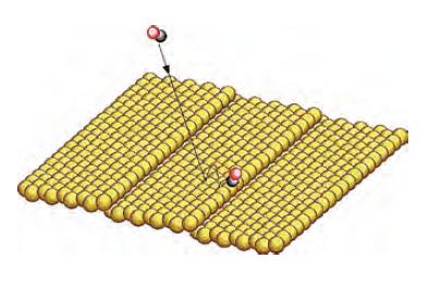 一酸化炭素分子の表面吸着過程
単原子ステップのあるプラチナ表面に一酸化炭素分子が吸着する際に,分子は 表面に到達してから0.7nm程度拡散する.
Adsorption process of CO on Pt surface
When a CO molecule is adsorbed on a stepped Pt surface, the mean lateral displacement from the first impact point to the final chemisorption site is about 0.7 nm.
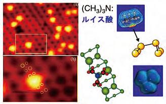 シリコン表面のトリメチルアミン分子
トリメチルアミン分子は,再構成したシリコン表面の負に帯電した原子の上に 選択的に吸着する.
Trimethylamine molecules on Si surface
A trimethylamine molecule is adsorbed at a positively charged specific site of the reconstructed Si surface.