
Quantum Hall Transport in Graphene Junctions
Osada Group
The electronic system of graphene can be regarded as a two-dimensional massless Dirac fermion system in solids resulting in remarkable relativistic behaviors. For example, carriers in graphene can never be confined by any potential barriers because of the Klein tunneling property. So, it is expected that graphene junctions, where two graphene systems under different potential touch with each other, show characteristic transport properties. In fact, the quantum Hall transport across the p-n bipolar junction of monolayer graphene have attracted much attention because of its fractional quantization of two-terminal conductance.
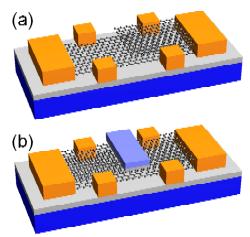
Fig.1. (a) Monolayer-bilayer heterojunction device of graphene. (b) p-n-p double bipolar junction device of bilayer graphene.
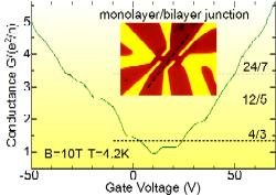
Fig.2. Gate voltage dependence of two-terminal conductance of the monolayer-bilayer hetero-junction device of graphene. Dotted lines indicate the plateau heights predicted by Landauer-Buttiker picture assuming full-mixing of edge states.
We have studied the quantum Hall transport of two other graphene junctions, the monolayer-bilayer hetero-junctions and the p-n bipolar junctions of bilayer graphene, for the first time (Fig. 1). In the quantum Hall state, two regions in both sides of the junctions have different quantum Hall indices (Chern numbers). Therefore, there should exist metallic states along the boundary between these regions. The purpose of research is to clarify the contribution of these boundary states to the quantum Hall transport.
The monolayer-bilayer graphene heterojunctions are interesting systems because of its pseudo-spin selectivity. To study quantum Hall transport in this system, we have used junctions formed accidentally in mechanical exfoliation on SiO2/n-Si substrate, which works as a gate electrode. As a function of gate voltage, the two-probe conductance across the monolayer-bilayer boundary shows the "V"-shaped characteristics with the staircase-like modulation corresponding to the Shubnikov-de Haas effect in both regions (Fig.2). The plateau heights of the staircase seem to almost coincides with fractional multiple of e2/h. This result has been considered using the Landauer-Buttiker formalism of edge channel transport in the quantum Hall state, which was also applied to the p-n junction of monolayer graphene. The observed result can be well explained by assuming full-mixing of edge states at the monolayer-bilayer boundary. This means that carriers in any input edge channels are distributed to all output channels with equal transmission probability.
Bilayer graphene is promising for device application because its energy gap can be controlled by external electric fields. The p-n bipolar junctions of bilayer graphene can be realized by the FET structure with an additional top gate electrode covering the sample partially. In this case, the top gate voltage does not only changes the potential of the gated region, but also opens the energy gap in the gated region. In the quantum Hall state, this energy gap breaks the degeneracy of the n=0 Landau level causing the n=0 quantum Hall plateau forbidden in the zerogap case. Therefore, we can expect interplay of quantum Hall transport and opening of the energy gap (namely, appearance of the n=0 quantum Hall state) in the partially gated bilayer. We have measured the two-terminal resistance of p-n-p double junctions of bilayer graphene as a function of top- and back-gate voltage. The resistance plateaus exhibit diamond-like pattern on the top- and back-gate voltage plane similar to that observed in p-n junctions of monolayer. The remarkable difference is the existence of high resistance regions along the charge neutral line of the top-gated region at high gate voltages. It corresponds to the appearance of the n=0 quantum Hall state. The observed plateau values can be almost explained by Landauer-Buttiker picture assuming full mixing of edge states along the p-n junction.