CEO growth: 1-25-01.2 (110) 5nm GaAs (490C growth) annealed at 600C for 10min
Substrate:12-18-00.1 position3 (GaAs (001) wafer)
Note: In position 1.3.5 of MBE chamber dated 1-25-01, substrate 12-18-00.1 was used
and another substrate 1-3-1.1 in 2,4 position: i.e. two substrate was used in the same first growth.
Yoshitasan named sample in alphabet order with the simplified growth name "b6" after sample growth position.
Accordingly this AFM sample observed by Oh, b6-c corresponds to position 3 sample in CEO growth, 1-25-01.2
using substrate 12-18-00.1.
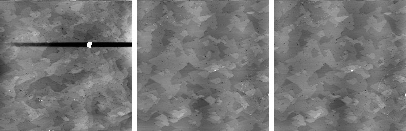
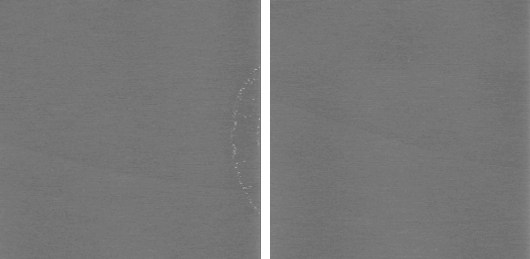
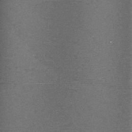
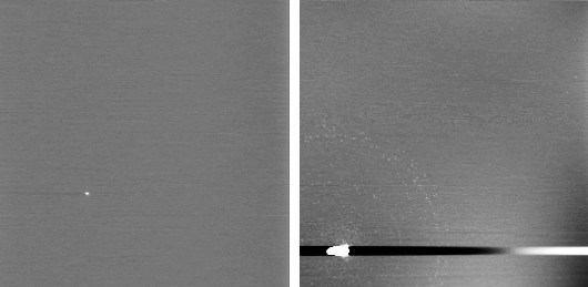
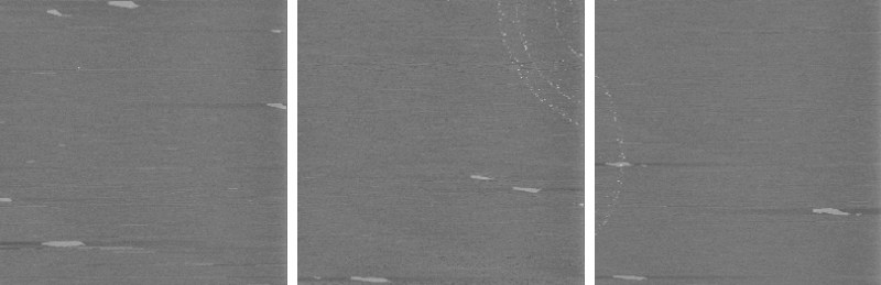
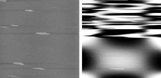
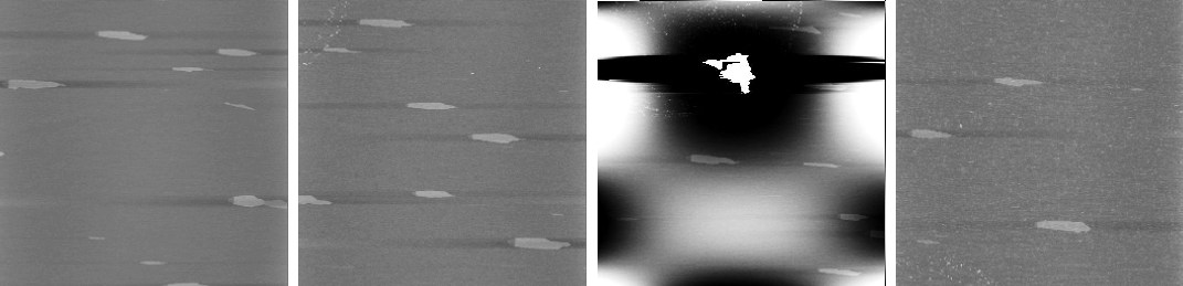
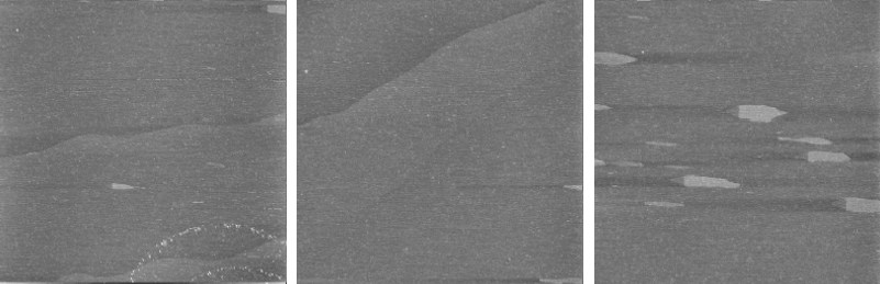
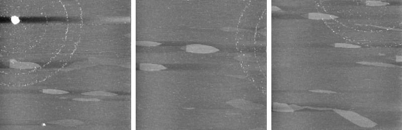
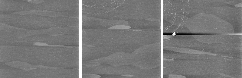
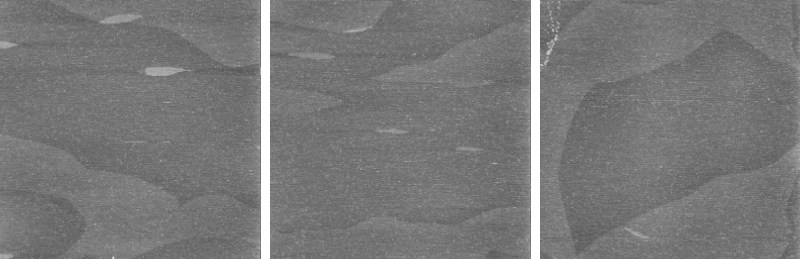
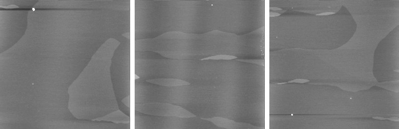
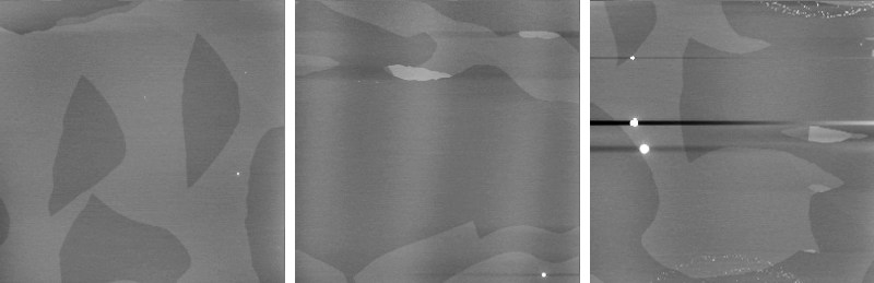
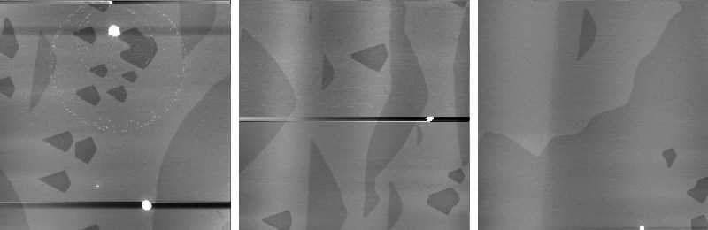
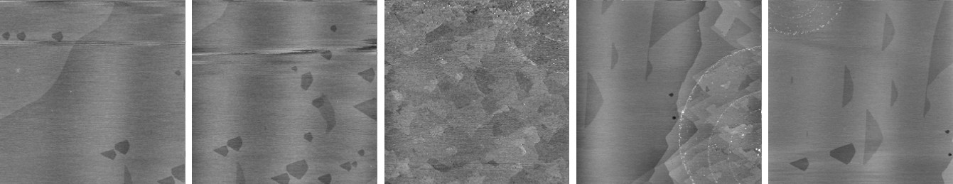
AFM Measurement Name: p3 scan (May 2002) and x scan (Rescan of same b6-c in May 2002) by Ji-Won Oh
in Akiyama-Lab
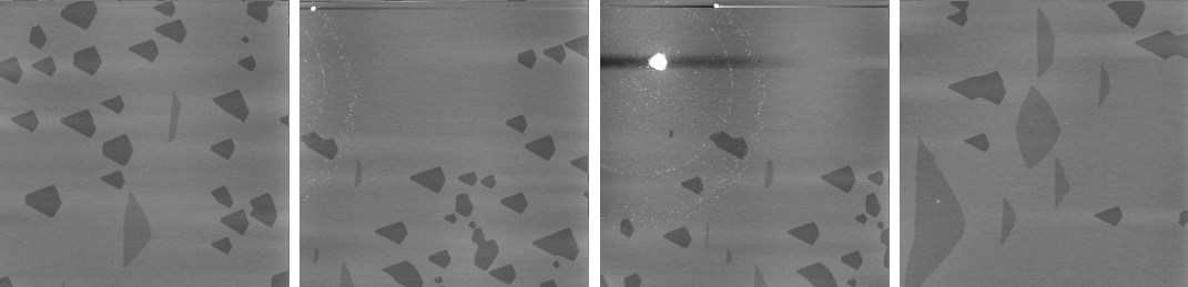
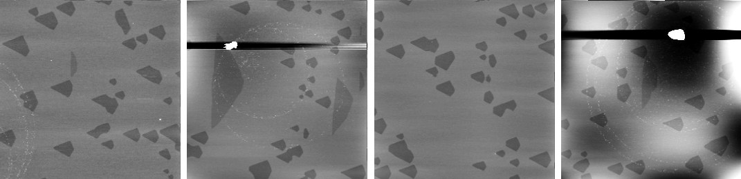
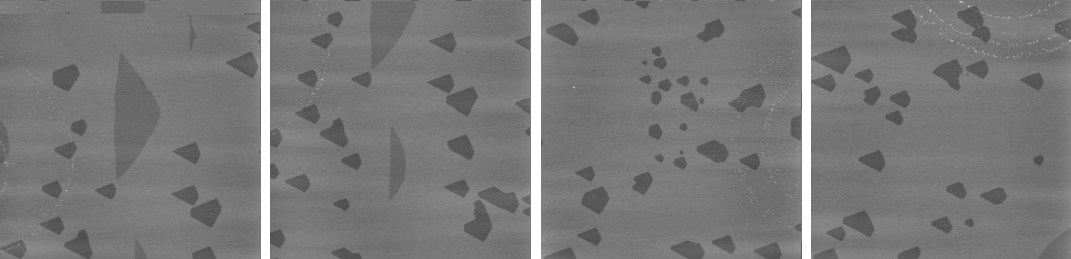
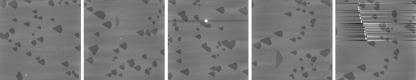
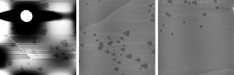
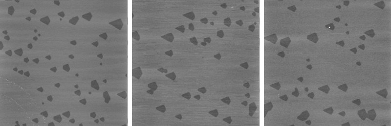
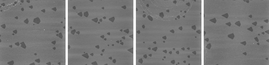
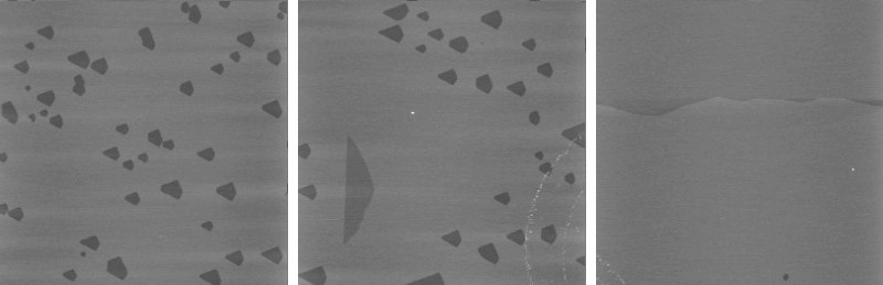
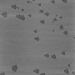
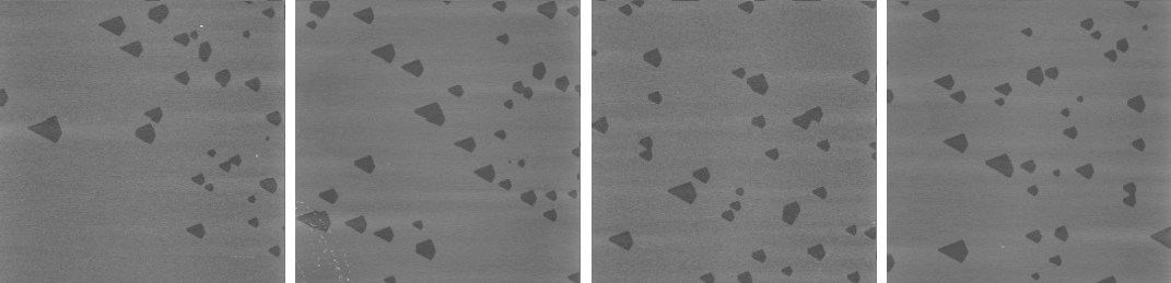
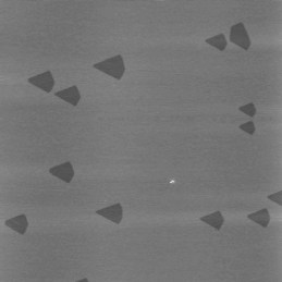
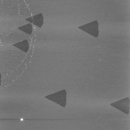
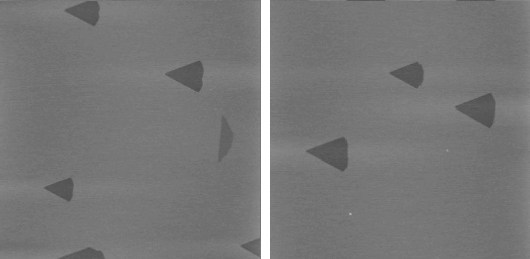
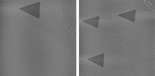
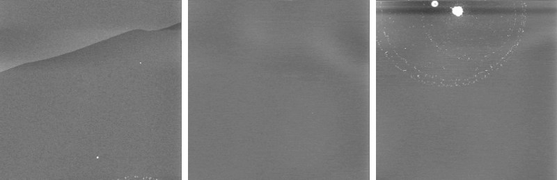
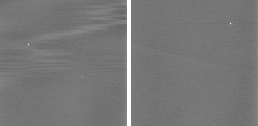
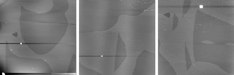
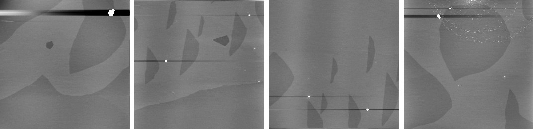
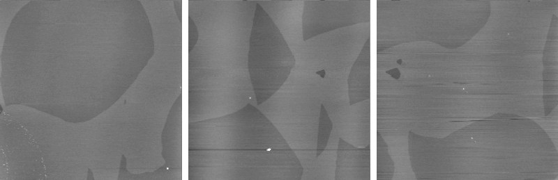
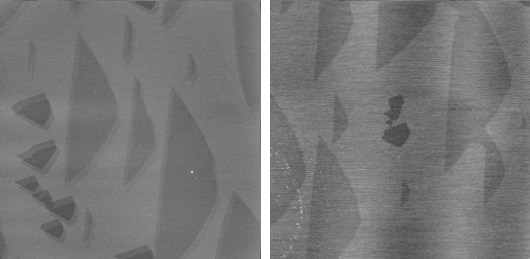
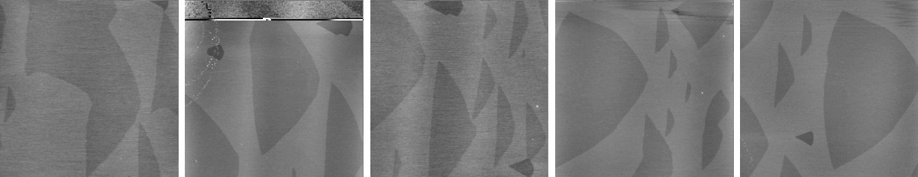
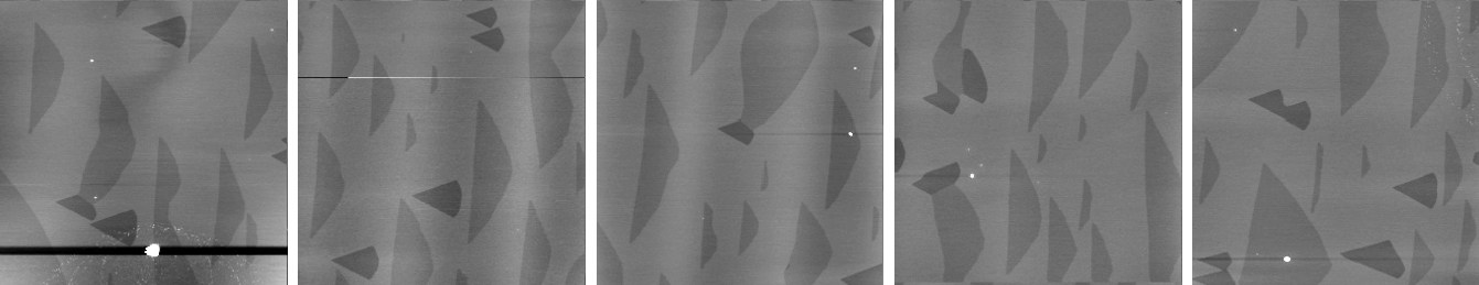
Meaurement Area: 5 mmx 5 mm
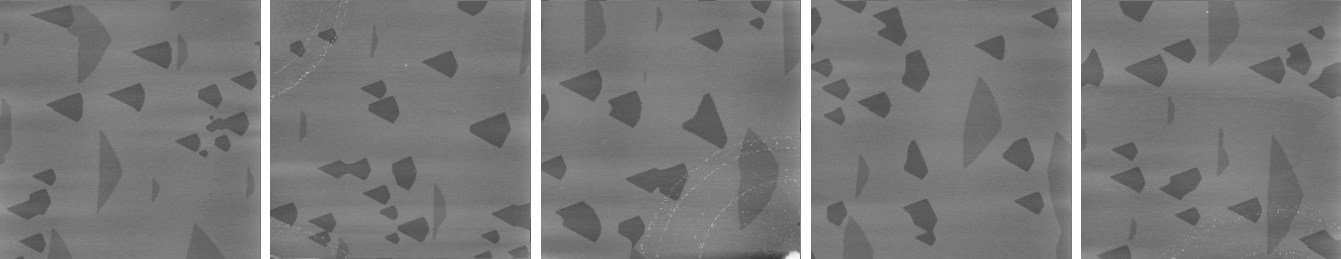
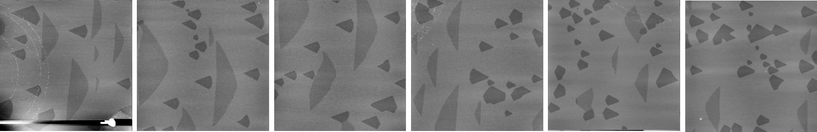
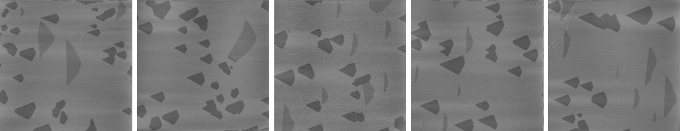
Left:FRONT (001)------Rght BACK (001)
Top: Thick GaAs-------Bottom: Thin GaAs ------- 1%/mm or 0.3 ML/mm ( 6nm of first growth , 0.06nm/mm coverage gradient; 1ML (GaAs110)=0.2nm)
The surplus or minus ML was caluclated based on above coverage assumption as to integer ML (P3-12).
Position Scan num. ML deviation
0.2 mm P3-33 -0.273 ML
0.3 mm P3-32 -0.27 ML
0.5 mm P3-31 -0.264 ML
1.1 mm P3-30 -0.246 ML
1.8 mm P3-29 -0.225 ML
2.5 mm P3-28 -0.204 ML
3 mm P3-27 -0.189 ML
3.4 mm P3-26 -0.117 ML
4.4 mm P3-25 -0.147 ML
4.9 mm P3-24 -0.132 ML
5.4 mm P3-23 -0.117 ML
6 mm P3-22 -0.099 ML
6.2 mm P3-21 -0.093 ML
6.5 mm P3-20 -0.084 ML
7 mm P3-19 -0.069 ML
7.2 mm P3-18 -0.063 ML
7.4 mm P3-17 -0.057 ML
7.5 mm P3-16 -0.054 ML
8.1 mm P3-15 -0.036 ML
8.5 mm P3-14 -0.024 ML
8.9 mm P3-13 -0.012 ML
9.3 mm P3-12 0 ML
9.7 mm P3-11 0.012 ML
10.5 mm P3-10 0.036 ML
10.6 mm P3-09 0.039 ML
11.2 mm P3-08 0.057 ML
11.9 mm P3-07 0.078 ML
12.5 mm P3-06 0.096 ML
13.6 mm P3-05 0.129 ML
15.6 mm P3-04 0.189 ML
18.1 mm P3-03 0.264 ML
21.7 mm P3-02 0.372 ML
23.3 mm P3-01 0.42 ML
24.2 mm X-12 0.447 ML
25.2 mm X-11 0.477 ML
26.6 mm X-10 0.519 ML
28 mm X-09 0.561 ML
28.5 mm X-08 0.576 ML
30.5 mm X-07 0.636 ML
31 mm X-06 0.651 ML
32.2 mm X-05 0.687 ML
32.8 mm X-04 0.705 ML
33.4 mm X-03 0.723 ML
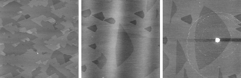
33.9 mm X-02 0.738 ML
35.2 mm X-01 0.777 ML